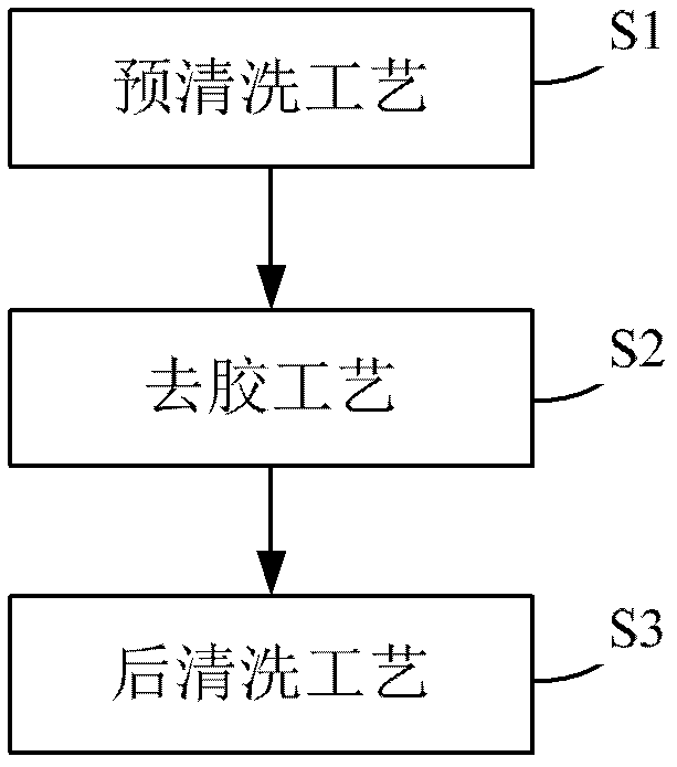
Deglue method for high aspect ratio structures
A high-to-width ratio, degumming technology, used in electrical components, semiconductor/solid-state device manufacturing, circuits, etc., can solve the problems of groove morphology, uncontrollable process factors, production cost and uneconomical efficiency, etc. Improves contact performance, avoids degumming residues, and improves degumming effect
- Summary
- Abstract
- Description
- Claims
- Application Information
AI Technical Summary
Problems solved by technology
Method used
Image

Examples
Embodiment 1
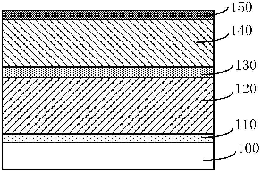
[0038] This embodiment is a deglue method for a DD structure using a conventional CMOS process, and the DD structure is a dual damascene structure including via holes and trenches. Figure 2A-2C It is a schematic cross-sectional structure diagram of the device corresponding to each step in the glue removal method of this embodiment.
[0039] First, if Figure 2A As shown, a substrate 100 is provided, and an etching stop layer 110, a first dielectric layer 120, an intermediate stop layer 130, a second dielectric layer 140, and an antireflection layer 150 are sequentially formed on the substrate 100; After the accumulation is completed, it can be formed as Figure 2A The five-layer structure shown.
[0040] Wherein, the substrate 100 can be such as silicon dioxide (SiO 2 ) dielectric layer, or a substrate with previous process graphics. The material of the etch stop layer 110 can be silicon nitride (Si 3 N 4 ), carbon-doped silicon nitride (NDC), etc., the thickness of the...
Embodiment 2
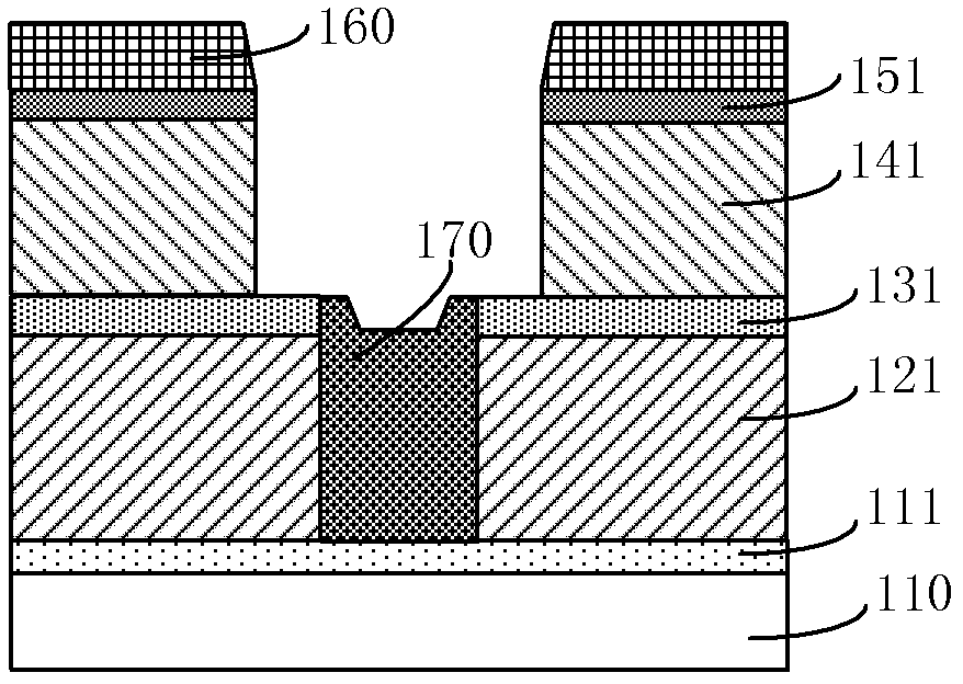
[0052] The present embodiment is a method for removing glue after etching pads in a specific pattern, and the specific pattern includes etched pads and grooves with different line widths filled with photoresist. Figure 3A-3C It is a schematic cross-sectional structure diagram of the device corresponding to each step in the glue removal method of this embodiment.
[0053] Such as Figure 3A In the device structure shown, 200 is the pressure point pattern after etching, 210 is the remaining photoresist, 220, 230, and 240 are dielectric layer grooves with different line widths, and the line widths are 1.5 μm and 3 μm respectively. , 6 μm, since the dielectric layer groove does not need to be etched and is filled with photoresist, its filling depth is 4-6 μm, preferably 5 μm here, and the remaining photoresist on the surface of the dielectric layer groove after the etching is completed The thickness is 2 μm. Therefore, the total thickness of the photoresist used for trench filli...
PUM
 Abstract
Description
Claims
Application Information
 - R&D
- Intellectual Property
- Life Sciences
- Materials
- Tech Scout
- Unparalleled Data Quality
- Higher Quality Content
- 60% Fewer Hallucinations
Browse by: Latest US Patents, China's latest patents, Technical Efficacy Thesaurus, Application Domain, Technology Topic, Popular Technical Reports.
© 2025 PatSnap. All rights reserved.Legal|Privacy policy|Modern Slavery Act Transparency Statement|Sitemap|About US| Contact US: help@patsnap.com