Back contact crystal silicon solar battery and manufacture process of back contact crystal silicon solar battery

A solar cell and manufacturing process technology, applied in the direction of circuits, photovoltaic power generation, electrical components, etc., can solve the problems of increasing series resistance, cost increase, and affecting battery efficiency, so as to increase short-circuit current density, improve battery efficiency, and reduce pollution Effect

Inactive Publication Date: 2012-07-25
XINGSHANG PHOTOVOLTAIC TECH SUZHOU
View PDF7 Cites 17 Cited by
  • Summary
  • Abstract
  • Description
  • Claims
  • Application Information

AI Technical Summary

Problems solved by technology

[0004] In the design of back-contact cells, EWT (emitter warp through) and MWT (metal warp through) are the main design prototypes. The completely grid-free design on the front side can maximize the use of the light-receiving surface, and at the same time, all the positive and negative electrodes are moved to the back side. However, the back side has PN-type regional characteristics at the same time, and due to the existence of parasitic capacitance effects, conventional aluminum back field passivation or high-density positive c...

Method used


Image

  • Back contact crystal silicon solar battery and manufacture process of back contact crystal silicon solar battery
  • Back contact crystal silicon solar battery and manufacture process of back contact crystal silicon solar battery
  • Back contact crystal silicon solar battery and manufacture process of back contact crystal silicon solar battery

Examples


Embodiment Construction

[0036] The present invention will be further described below in conjunction with the accompanying drawings.

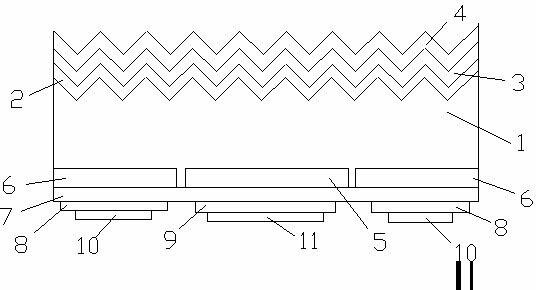
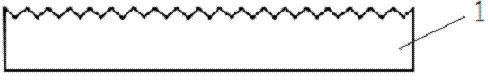
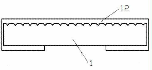
[0037] Such as figure 1 As shown, a back-contact crystalline silicon solar cell includes an N-type monocrystalline silicon wafer 1, the front side of the N-type monocrystalline silicon wafer 1 is provided with a first N-type heavily doped layer 2; The second N-type heavily doped layer 6 and the P-type heavily doped layer 5, the first N-type heavily doped layer 2 is provided with the first SiO 2 Passivation layer 3 and anti-reflection film layer 4, the second N-type heavily doped layer 6 and P-type heavily doped layer 5 are provided with a second silicon dioxide passivation layer 7, the second N-type heavily doped layer The second SiO at doped layer 6 2 The passivation layer 7 is provided with a heavily doped AZO thin film layer 8 and silver paste 10 in sequence; the second SiO at the P-type heavily doped layer 5 2 The passivation layer 7 is provided with a heavily d...


PUM

PropertyMeasurementUnit
Thicknessaaaaaaaaaa

Abstract

The invention discloses a back contact silicon solar battery, which comprises an N type monocrystalline silicon piece subjected to surface texturing, wherein a first N type heavy doping layer is arranged at the front side of the N type monocrystalline silicon piece, a silicon dioxide (SiO2) passivation layer and a reflection reduction film layer are sequentially arranged at the outer side of the first N type heavy doping layer, a second N type heavy doping layer and a P type heavy doping layer are arranged at the back side of the N type monocrystalline silicon piece in a mutual separating way, second SiO2 passivation layers are arranged at the outer side of the second N type heavy doping layer and the P type heavy doping layer, a heavy doping AZO film layer and silver slurry are sequentially arranged outside the second SiO2 passivation layer arranged at the second N type heavy doping layer part, and a heavy doping CuAlO2 film layer and silver aluminum slurry are sequentially arranged outside the second SiO2 passivation layer arranged at the P type heavy doping layer part. The invention also discloses a manufacture process of the back contact silicon solar battery. The back contact silicon solar battery and the manufacture method solve the problems that in the prior art, the conversion rate of the solar battery is low, and the back contact battery generally adopts laser punching, so the manufacture cost is high. Through the technical improvement, heavy doping is realized on the contact surface, the heavy-doping low-resistance transparent conductive oxide (TCO) materials are attached to the contact surface so as to form tunnel current, and in addition, a low-temperature slurry sintering method is adopted, the manufacture cost is reduced on the premise that the battery efficiency is ensured.

Description

technical field [0001] The invention relates to a back-contact crystalline silicon solar cell and a manufacturing process thereof, and belongs to the technical field of new solar cells. Background technique [0002] When sunlight hits a solar cell, the incident energy can be converted directly into electricity without mechanical rotation or polluting by-products. Solar cells are no longer the only treasures in the laboratory, and have been used for more than 50 years. What started out as providing power in space has now taken an increasing share of power generation on the ground. In recent years, the manufacturing technology of such batteries has been further improved. The production cost of solar cells will approach the level of thermal power generation, making a huge contribution to the world's energy demand. [0003] Among solar cells with various morphological structures, the back-contact crystalline silicon solar cell greatly reduces or even completely eliminates the...

Claims


Application Information

Patent Timeline
IPC IPC(8): H01L31/068H01L31/0224H01L31/0352H01L31/0216H01L31/18
CPCH01L31/022441H01L31/0682Y02E10/547
Inventor 殷晏庭王艳
Owner XINGSHANG PHOTOVOLTAIC TECH SUZHOU
Why Eureka
Try Eureka