Preparation method of organic thin-film field effect transistor

A field effect transistor and organic thin film technology, applied in the field of semiconductor field effect transistor device preparation, can solve the problems of affecting device performance, high cost of printing equipment, extremely demanding physical and chemical properties, etc., to achieve strong water and oxygen resistance, environmental protection The effect of loose, simplified process

Inactive Publication Date: 2012-07-25
SUZHOU INST OF NANO TECH & NANO BIONICS CHINESE ACEDEMY OF SCI
View PDF3 Cites 5 Cited by
  • Summary
  • Abstract
  • Description
  • Claims
  • Application Information

AI Technical Summary

Problems solved by technology

However, the disadvantages of using printing to form a film are that the physical and chemical properties such as ink viscosity and surface tension are extremely demanding, and at the same time, the cost of printing equipment itself is high, and low-cost production in the true sense has not been realized.
In addition, whether it is spin-coating, LB or printing, the solvents and substrates used in these methods are extremely sensitive to the quality of the film. For example, the volatilization rate, the surface energy of the substrate, etc. affect the crystallinity and The phase separation of the two-phase mixture will have a large impact, which in turn will affect the performance of the device
Some even require expensive printing equipment, making it difficult to achieve low-cost, large-area production

Method used


Image

  • Preparation method of organic thin-film field effect transistor
  • Preparation method of organic thin-film field effect transistor
  • Preparation method of organic thin-film field effect transistor

Examples


Embodiment 1

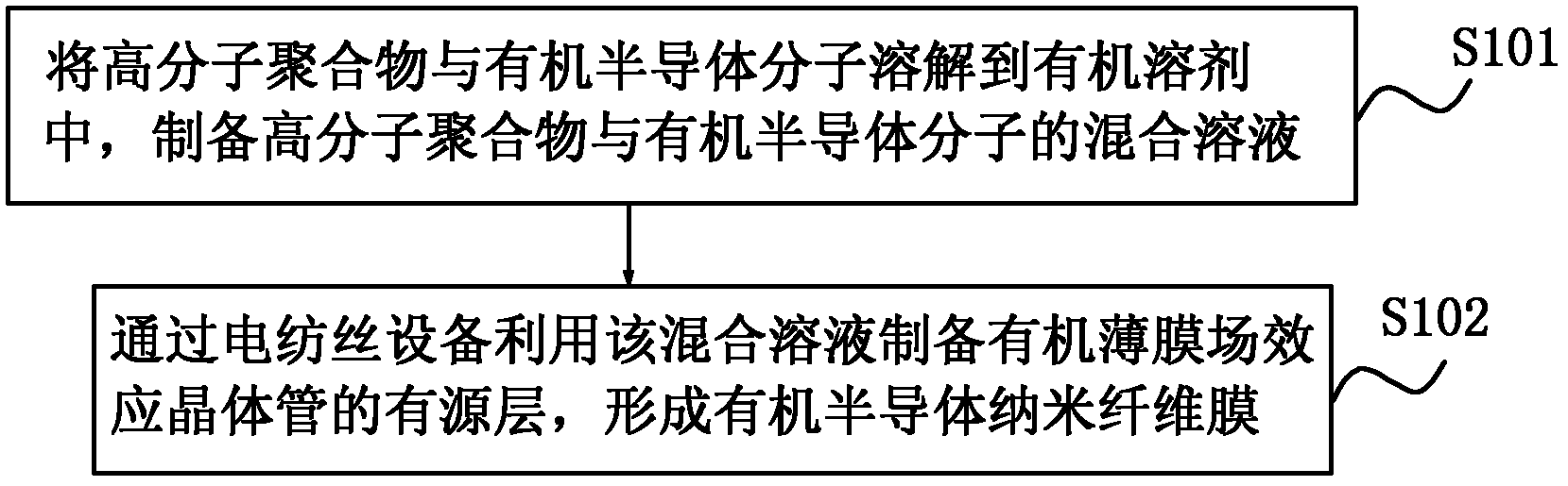
[0034] see figure 1 , figure 2 , Figure 5 with Figure 7 ,Such as figure 1 As shown, the method for preparing an organic thin film field effect transistor provided in this embodiment includes:

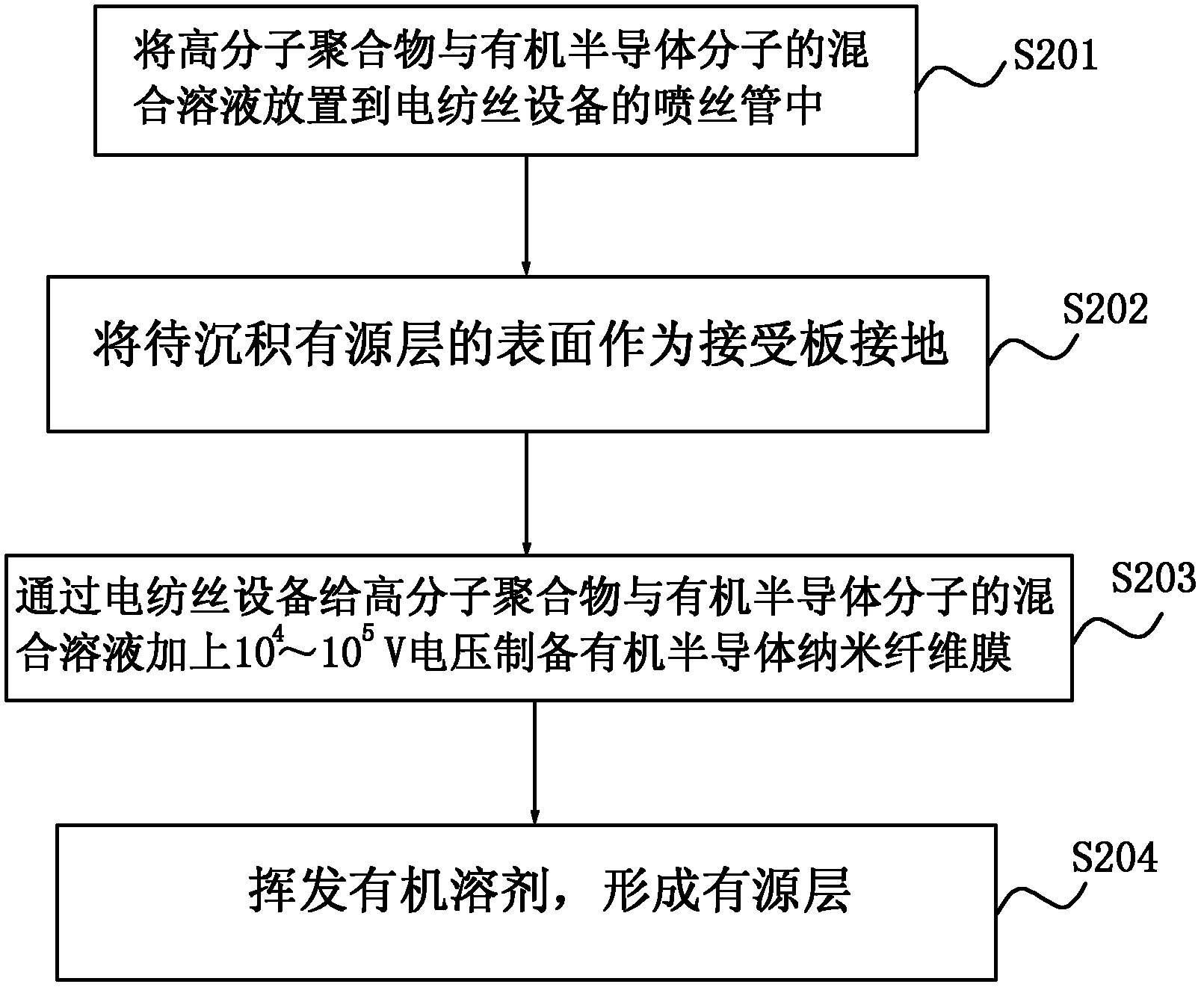
[0035] S101, dissolving the high molecular polymer and the organic semiconductor molecule into an organic solvent to prepare a mixed solution of the high molecular polymer and the organic semiconductor molecule;

[0036] S102, using the mixed solution to prepare an active layer of an organic thin film field effect transistor through an electrospinning device to form an organic semiconductor nanofiber film.

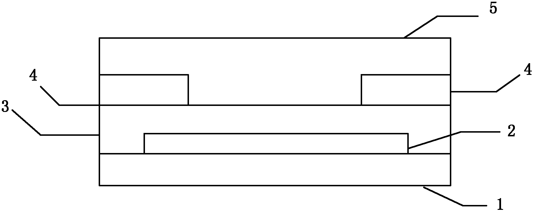
[0037] Among them, such as Figure 5 As shown, the field effect transistor of this embodiment includes a substrate 1 , a gate electrode 2 , an insulating layer 3 , source and drain electrodes 4 and an active layer 5 . Wherein, the substrate 1 is a glass material, and the mixed solution is prepared by stirring the mixed solution of the polymer and the organic semiconductor m...

Embodiment 2

[0048] see figure 1 , figure 2 , Figure 4 with Figure 7 ,Such as figure 1 As shown, the method for preparing an organic thin film field effect transistor provided in this embodiment includes:

[0049] S101, dissolving the high molecular polymer and the organic semiconductor molecule into an organic solvent to prepare a mixed solution of the high molecular polymer and the organic semiconductor molecule;

[0050]S102, using the mixed solution to prepare an active layer of an organic thin film field effect transistor through an electrospinning device to form an organic semiconductor nanofiber film.

[0051] Among them, such as Figure 4 As shown, the field effect transistor of this embodiment includes a substrate 1 , a gate electrode 2 , an insulating layer 3 , source and drain electrodes 4 and an active layer 5 . Wherein, the substrate 1 is a ceramic material. In this embodiment, the method for preparing the mixed solution is to stir the mixed solution of the high molec...

Embodiment 3

[0062] see figure 1 , 2 , 5, 7, such as figure 1 As shown, the method for preparing an organic thin film field effect transistor provided in this embodiment includes:

[0063] S101, dissolving the high molecular polymer and the organic semiconductor molecule into an organic solvent to prepare a mixed solution of the high molecular polymer and the organic semiconductor molecule;

[0064] S102, using the mixed solution to prepare an active layer of an organic thin film field effect transistor through an electrospinning device to form an organic semiconductor nanofiber film.

[0065] Among them, such as Figure 5 As shown, the field effect transistor of this embodiment includes a substrate 1 , a gate electrode 2 , an insulating layer 3 , source and drain electrodes 4 and an active layer 5 . Wherein, the substrate 1 is made of silicon. In this embodiment, the method of preparing the mixed solution is to stir the mixed solution of the high molecular polymer and the organic semi...


PUM


Abstract

The invention discloses a preparation method of an organic thin-film field effect transistor. The preparation method comprises the following steps of: dissolving a mixture of a high polymer and molecules of an organic semiconductor in an organic solvent for forming a mixed solution; and then spraying the mixed solution into a trench between a source electrode and a drain electrode through an electrospinning device to form an organic semiconductor nano-fiber membrane as an active layer of the organic thin-film field effect transistor. The large-scale production of low-cost and large-scale nano-size high-efficient organic thin-film field effect transistors can be realized through an electrospinning technology. Simultaneously, the requirements for environments required for the preparation method are very low, the preparation method does not need to be implemented in a glove box and other anhydrous and anoxybiotic environments, and the process is simplified; and furthermore, a prepared organic electronic device has very strong resistance to water oxygen, and the preparation method of the active layer membrane is well improved to get a high-performance field effect transistor.

Description

technical field [0001] The invention relates to a preparation method of a semiconductor field effect transistor device, in particular to a preparation method of an organic thin film field effect transistor and a mixed solution of an organic semiconductor molecule and a high molecular polymer. Background technique [0002] Organic field-effect transistors have attracted extensive research interest due to their potential applications in flexible displays, organic integrated circuits, and electronic identification. In recent years, organic field effect transistors have made great progress in the design and synthesis of new stable organic semiconductor materials and device preparation. [0003] It is well known that the main factor determining the performance of organic field effect transistors is the structure and morphology of the active layer film. At present, the processes for preparing OFET active layer thin films are mainly vacuum coating, photolithography, electron beam ...

Claims


Application Information

Patent Timeline
Patent Type & Authority Applications(China)
IPC IPC(8): H01L51/40H01L51/05
Inventor 潘革波肖燕
Owner SUZHOU INST OF NANO TECH & NANO BIONICS CHINESE ACEDEMY OF SCI
Why Eureka
Try Eureka