Nano grating mask preparation method for surface plasma photoetching

A technology of surface plasmon and nano-grating, which is applied in the photoplate-making process of patterned surface, optical mechanical equipment, optics, etc., can solve the problems of difficult preparation of grating, difficult preparation, high price, etc., and achieve the effect of reducing costs

Active Publication Date: 2012-08-08
INST OF OPTICS & ELECTRONICS - CHINESE ACAD OF SCI
4 Cites 5 Cited by

AI-Extracted Technical Summary

Problems solved by technology

The main methods of lithography include optical exposure, electron beam exposure, X-ray exposure, etc. Due to the diffraction effect of light and electron scattering problems in electron beam exposure, it is difficult to prepare gratings with a period below 60nm; X-ray exposure is due to the small It is very difficult to prepare a mask with a large line width, and it is not suitable for the preparation of gratings with a period below 60nm
The direct writing methods main...

Abstract

The invention provides a nano grating mask preparation method for surface plasma photoetching, which comprises the steps that: a grating array structure is prepared on a substrate; shadow evaporation of masking layer, RIE (Reactive Ion Etching) of substrate and removal of masking layer are carried out in the direction of one side of a grating line, and shadow evaporation of masking layer, RIE (Reactive Ion Etching) of substrate and removal of masking layer are carried out in the direction of the other side of the grating line; isotropic etching is carried out using RIE, or the grating line issubjected to isotropic wet etching through etchant, and the depth of RIE or wet etching is controlled to reduce the width of the grating line to a preset value; and shadow evaporation of masking layer, RIE (Reactive Ion Etching) of substrate and removal of masking layer are carried out in the direction of one side of the width-reduced fiber grating, and then shadow evaporation of masking layer, RIE (Reactive Ion Etching) of substrate and removal of masking layer are carried out in the direction of the other side of the width-reduced fiber grating. The lines obtained according to the method disclosed by the invention is four times as much as the lines of the previous grating, and grating period is reduced to one fourth of the previous grating period.

Application Domain

Photomechanical apparatus

Technology Topic

NanometreIsotropic etching +7

Image

  • Nano grating mask preparation method for surface plasma photoetching
  • Nano grating mask preparation method for surface plasma photoetching
  • Nano grating mask preparation method for surface plasma photoetching

Examples

  • Experimental program(4)

Example Embodiment

[0036] Embodiment 1, using a photoresist grating with a period of 200nm to fabricate a silicon grating array with a period of 50nm, the fabrication process is as follows:
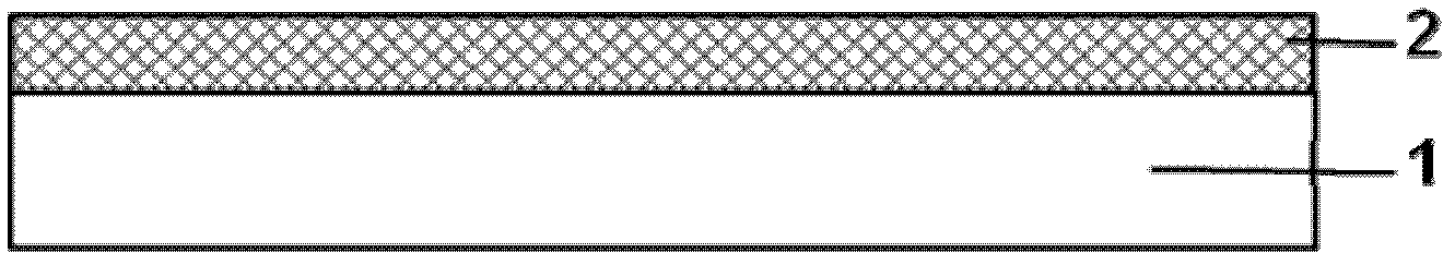
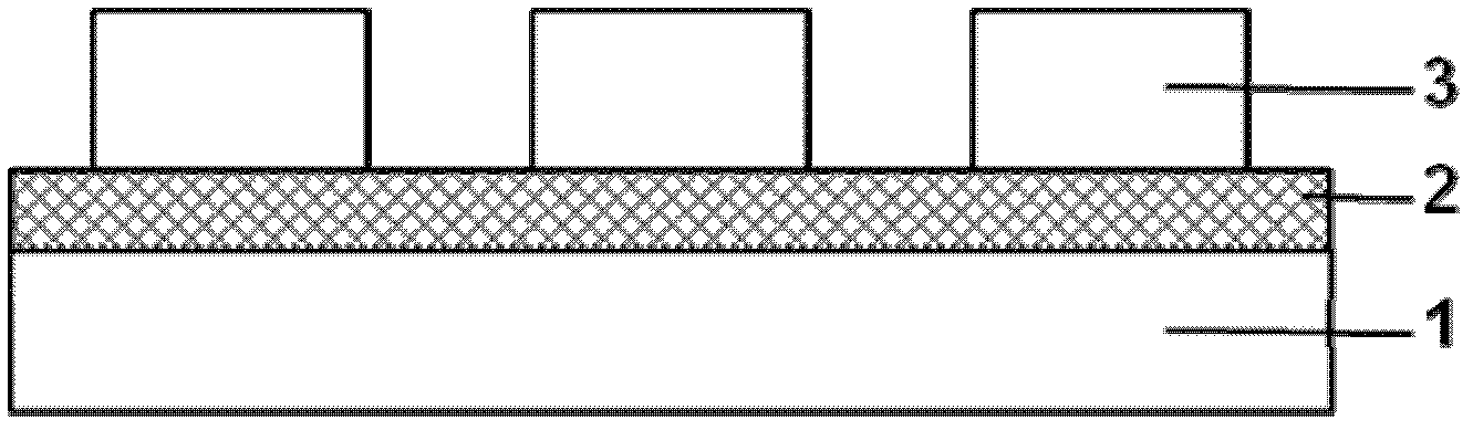
[0037] (1) Plating 50nm silicon on a quartz substrate, such as figure 1 As shown, then a grating array with a period of 200nm and a photoresist line width of 120nm is prepared on the substrate by an interference lithography method with a light source of 365nm laser, as figure 2 shown;
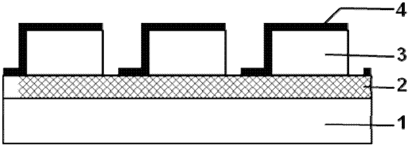
[0038] (2) Towards the right side of the grating lines, shadow evaporated chromium is used as a masking layer, and a narrow slit with a width of 30nm without a chromium masking film layer is obtained on the right side of each grating line, as image 3 shown;
[0039] (3) Use SF 6 The gas performs anisotropic RIE method to etch a 50nm silicon film layer, and it will stop when it reaches the quartz material, such as Figure 4 shown;
[0040] (4) Remove the chromium masking layer to obtain a group of narrow slit lines that are etched and transferred to the silicon film layer, such as Figure 5 shown;
[0041] (5) Then perform shadow vapor deposition of chromium masking layer, RIE etching, and removal of chromium masking layer to the other side of the grating line, and obtain the second set of narrow slit lines etched on the silicon film layer on the other side of the grating line ,like Figure 6-8 shown;
[0042] (6) Use 30Pa cavity pressure O 2 Carry out RIE isotropic etching, control the depth of RIE etching to reduce the width of grating lines to 20nm, such as Figure 9 shown;
[0043] (7) Perform shadow evaporation masking layer, RIE etching, and masking layer removal to the right side of the grating lines with reduced width to obtain the third group of narrow slit lines, such as Figure 10 shown; then shadow evaporation masking layer, RIE etching, and masking layer removal are performed on the other side of the grating lines with reduced width to obtain the fourth group of narrow slit lines, as shown in Figure 11 As shown; after removing the photoresist, four parallel lines can be obtained from each grating line, and the grating period is reduced from 200nm of the imprinted rubber grating to 50nm of the silicon grating array, such as Figure 12 shown.

Example Embodiment

[0044] Embodiment 2, a germanium grating array with a period of 40nm is produced with a photoresist grating with a period of 160nm, and the production process is as follows:
[0045] (1) Plating 40nm germanium on a glass substrate, then using a 257nm laser as a light source to carry out interference lithography, and preparing a photoresist grating array with a period of 160nm and a photoresist line width of 100nm on the substrate;
[0046] (2) Carry out shadow vapor deposition of copper as a masking layer to one side of the grating lines, and obtain a narrow slit with a width of 20nm without a copper masking film layer on the side of each grating line;
[0047] (3) Carry out the anisotropic RIE method to etch through the germanium film layer, and stop automatically when the glass material is etched;
[0048] (4) removing the copper masking layer to obtain a group of narrow slit lines that are etched and transferred to the germanium substrate;
[0049](5) Then perform shadow vapor deposition of copper masking layer, RIE etching, and removal of copper masking layer toward the other side of the grating line, and obtain a second set of slit lines etched on the substrate on the other side of the grating line;
[0050] (6) Use 30Pa cavity pressure O 2 Carry out RIE isotropic etching, control the depth of RIE etching to reduce the width of grating lines to 20nm;
[0051] (7) Perform shadow evaporation copper masking layer, RIE etching, and copper masking layer removal to the right side of the grating lines with reduced width to obtain the third group of narrow slit lines; then proceed in the direction of the other side of the reduced grating lines Shadow evaporation of copper masking layer, RIE etching, removal of copper masking layer to obtain the fourth group of narrow slit lines; after removing the photoresist, four parallel lines can be obtained from each grating line, and the grating period is determined by the photoresist grating The 160nm shrinks to the 40nm of the germanium grating array.

Example Embodiment

[0052] Example 3, an aluminum grating array with a period of 30nm is produced with an imprinted rubber grating with a period of 120nm, and the production process is as follows:
[0053] (1) Plating 30nm of aluminum on a flat copper substrate, and then preparing a grating array with a period of 120nm and an embossing glue line width of 75nm on the substrate by a nanoimprint method;
[0054] (2) Towards the right side of the grating lines, shadow evaporated silver is used as a masking layer, and a narrow slit with a width of 15nm without silver masking film layer is obtained on the right side of each grating line;
[0055] (3) Carry out anisotropic RIE method to etch the aluminum film layer of 30nm;
[0056] (4) remove the silver masking layer to obtain a group of slit lines that are etched and transferred to the aluminum film layer;
[0057] (5) Then shadow evaporate the silver masking layer, RIE etching, and remove the silver masking layer to the other side of the grating line, and obtain the second set of narrow slit lines etched on the aluminum film layer on the other side of the grating line strip;
[0058] (6) Use NF with 20Pa cavity pressure 3 Carry out RIE isotropic etching, control the depth of RIE etching to reduce the width of grating lines to 15nm;
[0059] (7) Perform shadow evaporation masking layer, RIE etching, and removal of the masking layer to the right side of the reduced-width grating lines to obtain the third group of narrow slit lines; then perform shadow evaporation in the direction of the other side of the reduced-width grating lines Plating a masking layer, RIE etching, and removing the masking layer to obtain the fourth group of narrow slit lines; after removing the photoresist, four parallel lines can be obtained from each grating line, and the grating period is reduced from 120nm of the embossed rubber grating to 30nm of aluminum grating array.

PUM

PropertyMeasurementUnit
Width15.0nm
Width20.0nm

Description & Claims & Application Information

We can also present the details of the Description, Claims and Application information to help users get a comprehensive understanding of the technical details of the patent, such as background art, summary of invention, brief description of drawings, description of embodiments, and other original content. On the other hand, users can also determine the specific scope of protection of the technology through the list of claims; as well as understand the changes in the life cycle of the technology with the presentation of the patent timeline. Login to view more.

Similar technology patents

Magnetically guided catheter

ActiveUS20100174177A1low costhigh performance
Owner:ST JUDE MEDICAL ATRIAL FIBRILLATION DIV

Head mounted display with eye accommodation

InactiveUS20070097277A1low cost
Owner:UNIV OF CENT FLORIDA RES FOUND INC +1

Method for removing pollutants in sewage

InactiveCN103449680Alow costEasy to prepare
Owner:JIANGSU LV CHUAN ENVIRONMENTAL PROTECTION TECH

Classification and recommendation of technical efficacy words

  • low cost

System and method for transmitting wireless digital service signals via power transmission lines

ActiveUS7929940B1reduce bandwidth requirementlow cost
Owner:NEXTEL COMMUNICATIONS

Plastic waveguide-fed horn antenna

InactiveUS20100214185A1low cost
Owner:RGT UNIV OF CALIFORNIA

System and method for determination of position

InactiveUS20090149202A1low costreduce requirement
Owner:STEELE CHRISTIAN

Adaptive antenna optimization network

InactiveUS6961368B2low costminimal space
Owner:ERICSSON INC
Why Eureka
Try Eureka