Transfer preparation method of patterned graphene

A technology for patterning graphene and graphene, applied in the manufacture of semiconductor/solid-state devices, electrical components, circuits, etc., can solve the problems of graphene sample cracking, damage, solvent damage to the substrate, etc., to achieve the effect of keeping clean

Inactive Publication Date: 2012-08-15
LANZHOU UNIVERSITY
View PDF4 Cites 61 Cited by
  • Summary
  • Abstract
  • Description
  • Claims
  • Application Information

AI Technical Summary

Problems solved by technology

In the process of transferring graphene from the metal growth substrate to the target substrate, wet or dry transfer can be used. The wet transfer mainly uses the spin coating method to deposit PMMA or other colloidal films on the surface of graphene, and then uses chemical reagents to corrode. Metal substrate, to separate the graphene from the metal substrate, transfer the graphene to a new target substrate, and then use an organic solvent such as acetone or chloroform to dissolve the colloidal film to obtain a graphene sample, such as the surface of the target transfer substrate When other organic materials are attached, or the target substrate itself is easily damaged by organic solvents, the application of this method is limited; dry transfer mainly uses PDMS (polydimethylsiloxane) or other thermal decomposition tapes to directly press Printed on the surface of graphene as a dielectric material to protect graphene, and then use chemical reagents to separate graphene from the metal substrate, transfer graphene to a new target substrate, and then use mechanical methods to remove the PDMS protective film to obtain The final graphene sample, but this method is prone to cracking of the graphene sample
When graphene is patterned by ion beam etching, electron beam etching or laser beam etching, colloid is usually spin-coated on the surface of graphene as a mask. After etching, the colloid needs to be washed off with an organic solvent. , there is also solvent damage to the substrate, and the use of ion beams, electron beams or laser beams, such high-energy particles or beams, can damage organic material substrates, which are only suitable for inorganic material substrates such as silicon wafers and quartz.

Method used


Image

  • Transfer preparation method of patterned graphene
  • Transfer preparation method of patterned graphene

Examples


Embodiment 1

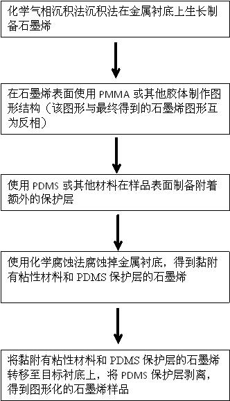
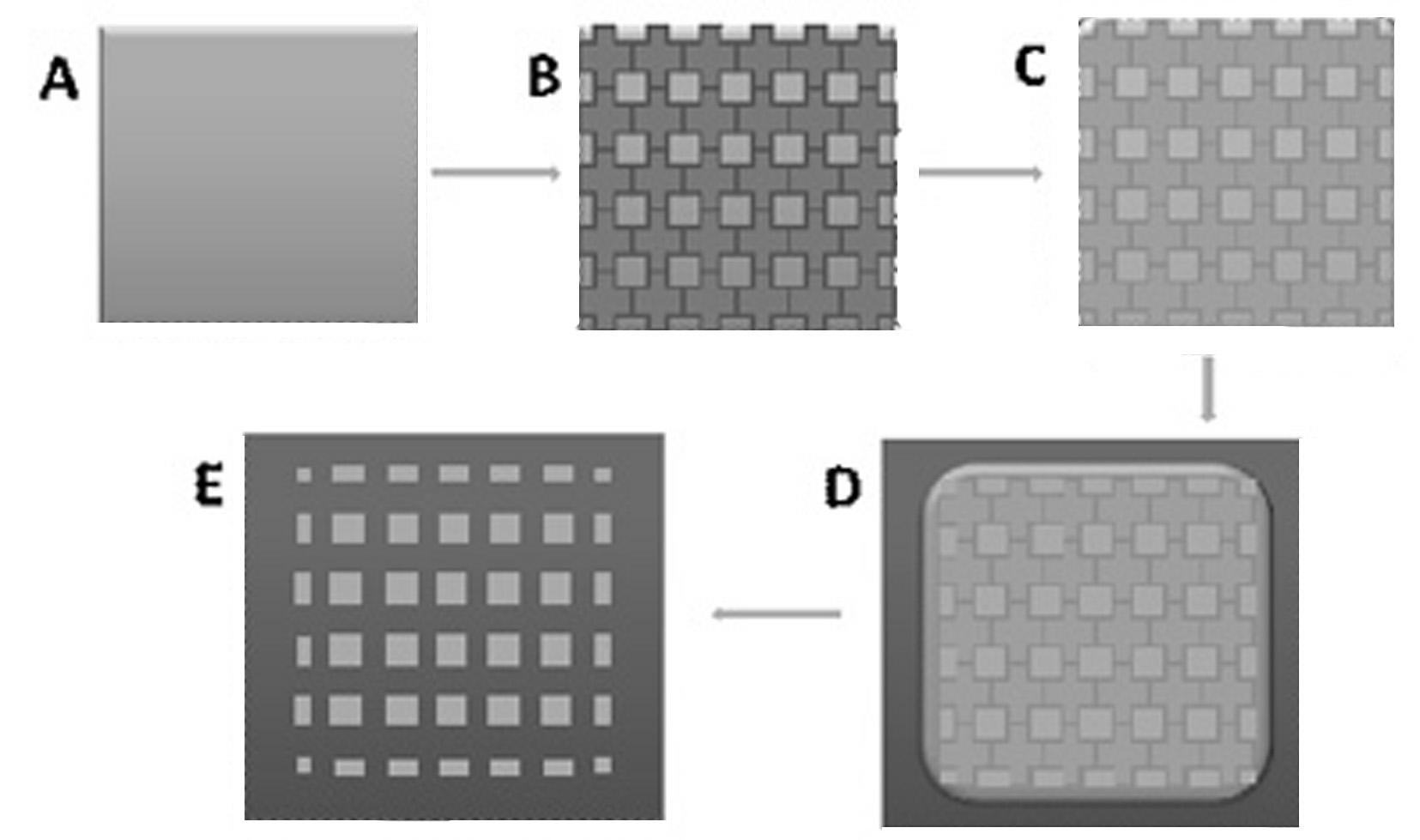
[0022] Use chemical vapor deposition to grow graphene on the surface of copper foil. The specific process: use hydrogen and methane as the gas source, place the copper foil in a tube furnace, heat the tube furnace to 1000 degrees Celsius in a vacuum environment, and feed The hydrogen of 2sccm and the methane of 35sccm and keep 15 minutes, turn off heating device, after the tube furnace is cooled to normal pressure, promptly grow the graphene of single layer on the surface of copper foil, as figure 2 a.

[0023] Use a glass fiber to dip a small amount of PMMA solution, and draw a grid-like structure on the surface of the graphene-grown copper foil. The size of the grid is about 1 mm, and the thickness of the grid lines is about 0.3 mm. Place the sample that has drawn the PMMA pattern in the air and let it stand for half an hour. After the solvent volatilizes, a patterned PMMA film is obtained on the graphene surface, such as figure 2 b. Printing or printing techniques can...


PUM


Abstract

The invention discloses a transfer preparation method of patterned graphene, which comprises the following steps: coating an adhesive material on a graphene surface, which grows on a catalytic metallic substrate, according to a designed pattern; coating a PDMS (polydimethylsiloxane) layer on the graphene surface, and thermosetting; soaking the obtained sample in an etching solution to remove the catalytic metallic substrate, so that the graphene with the adhesive material and the PDMS floats in the solution; transferring the graphene with the adhesive material and the PDMS onto a target substrate; and stripping the PDMS from the target substrate to obtain the patterned graphene. The method disclosed by the invention does not limit the use of materials of the target substrate; when stripping the PDMS, an expected pattern can be obtained without causing additional structure damage on the graphene, and meanwhile, the graphene surface is kept clean; and the invention can be used for preparing patterned graphene without expensive etching equipment.

Description

technical field [0001] The invention belongs to the field of nanometer materials and microelectronic devices, and in particular relates to a transfer preparation method of patterned graphene. Background technique [0002] Graphene is an emerging two-dimensional nanomaterial in recent years. Due to its excellent mechanical properties, light transmittance, thermal conductivity, and electrical conductivity, it can be used as a transparent electrode material in the fields of solar cells and touch panels in industry. , At the same time, it can also replace the current copper wire as the wire material of the integrated circuit. The preparation of graphene by chemical vapor deposition (CVD) on catalytic metal substrates (such as copper, nickel, etc.) is currently the main production method suitable for large-scale industrial applications. The graphene produced by this method must adopt a certain process Only by transferring graphene to the target substrate and making it into a spe...

Claims


Application Information

Patent Timeline
Patent Type & Authority Applications(China)
IPC IPC(8): H01L21/02H01L21/00
Inventor 耿柏松王枫闫鹏勋卓仁富吴志国王君闫德
Owner LANZHOU UNIVERSITY
Why Eureka
Try Eureka