Realization method for lead bonding thick aluminum wire

A realization method and wire bonding technology, applied in the manufacture of electrical components, electrical solid devices, semiconductor/solid devices, etc., can solve problems such as product reliability discount, cost increase, complex conditions, etc., and achieve simplification of welding equipment and production process Simplification and great electrical performance

Active Publication Date: 2012-08-15
SICHUAN LIPTAI ELECTRONICS
View PDF6 Cites 10 Cited by
  • Summary
  • Abstract
  • Description
  • Claims
  • Application Information

AI Technical Summary

Problems solved by technology

For the copper wire process, a certain cost can be saved on the basis of the gold wire, but the conditions required in the bonding process are more complicated, because the copper wire needs to be protected by a protective gas when performing bonding, which increases the cost and increases the cost. Difficulty of craft
Before copper wire welding, a copper ball needs to be sintered by electric current. Once the copper ball is oxidized, it is easy to leave craters on the aluminum layer of the chip, which will affect the quality of the product and greatly reduce the reliability of the product.
At the same time, similar to go

Method used


Image

  • Realization method for lead bonding thick aluminum wire
  • Realization method for lead bonding thick aluminum wire
  • Realization method for lead bonding thick aluminum wire

Examples


Embodiment Construction

[0047] The invention will be described in further detail below with reference to the embodiments of the accompanying drawings.

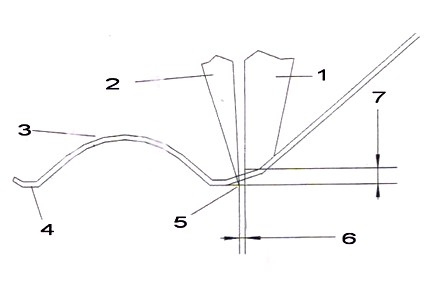
[0048] according to figure 1 When welding, adopt the method for realizing thick aluminum wire lead bonding of the present invention, and its operating conditions are as follows:

[0049] (1) Selection of rivets

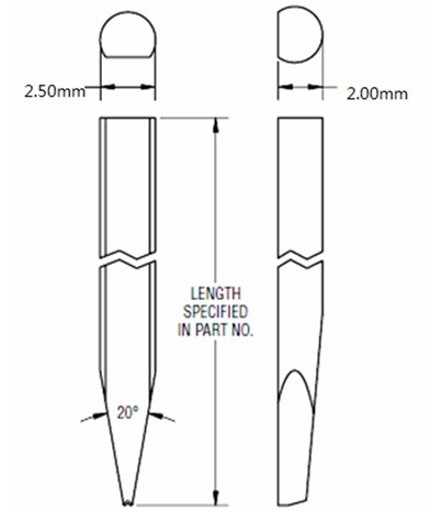
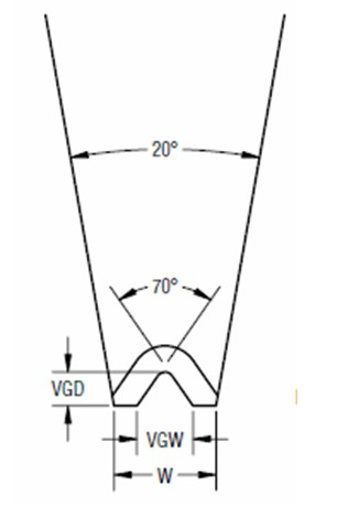
[0050] Due to the good ductility of aluminum wire, during the operation of the production line, it is easy to cause de-soldering when pulling the wire, and continuous operation cannot be performed. It is necessary to design a riving knife that matches the specifications of the thick aluminum wire diameter. , so as to ensure the smooth operation of the production line. There are several parts of the rivet that need to be modified, including T size, BL size, ER&BF size, H size, W size, VGW size; in addition, the choice of rivet material and surface finish ensures that the rivet has enough strength to complete The welding process is not easy...


PUM

PropertyMeasurementUnit
Thicknessaaaaaaaaaa
Thicknessaaaaaaaaaa
Thicknessaaaaaaaaaa

Abstract

The invention relates to the technical field of the semiconductor packaging, in particular to a realization method for lead bonding a thick aluminum wire. The method comprises the following four important operation key points of designing and optimizing a chopper, detecting chip surface aluminum layer thickness, optimizing and matching a bonding technical parameter, and detecting the bonding strength. As the thick aluminum wire is unlikely to oxidize, the production technology is simplified, and the cost can be obviously lowered. Meanwhile, the thick aluminum wire has the advantages of small contact resistance, low device power consumption, high bonding strength and the like. The chip aluminum layer thickness is detected by 85% phosphoric acid solution so as to ensure that the aluminum layer thickness is more than 5.0mum when the thick aluminum wire is lead bonded, and craters can be prevented from generating in the operation process. The technical parameter adopts initial power pressure, and the craters can be prevented by regulating the initial power pressure according to the practical situation. Whether the welding strength reaches the standard is judged by measuring the breaking force of the bonding wire by a gram force meter. According to the realization method for lead bonding the thick aluminum wire, the cost can be obviously lowered, the device power consumption is lowered, and the product reliability can be improved.

Description

technical field [0001] The invention relates to the technical field of semiconductor packaging, in particular to a method for realizing high-power Schottky, fast recovery and IGBT using thick aluminum wire wire bonding in semiconductor device packaging. Background technique [0002] Gold wire and copper wire wire bonding are the most widely used wire bonding technology in the electronics industry, but gold wire and copper wire cannot meet the bonding technical requirements of high-power devices, modules and IGBT products due to cost and welding process limitations. [0003] With the development of the semiconductor industry, the power of packaged devices has been greatly increased to meet the needs of the market. The improvement of device power involves the withstand voltage capability and current flux of the inner lead. The semiconductor packaging industry first adopted thick aluminum wires to replace the previously used gold wires and copper wires. Although the gold wire ...

Claims


Application Information

Patent Timeline
IPC IPC(8): H01L21/603H01L21/66
CPCH01L24/78H01L2224/05624H01L2224/45015H01L2224/45124H01L2224/45144H01L2224/45147H01L2224/48091H01L2224/48247H01L2224/48472H01L2224/48624H01L2224/48724H01L2224/48824H01L2224/78H01L2224/78313H01L2224/7855H01L2224/85H01L2924/00011H01L2924/12032H01L2924/13055H01L2924/00014H01L2924/00H01L2924/00012H01L2924/01004
Inventor 李科蔡少峰陈凤甫
Owner SICHUAN LIPTAI ELECTRONICS
Why Eureka
Try Eureka