Thin-film packaging component, photoelectronic device and packaging method of photoelectronic device

An optoelectronic device and thin film packaging technology, applied in the field of optoelectronics, can solve the problems of limiting the service life of OLEDs and the inability to use flexible flat-panel displays, and achieve the effects of reducing packaging costs, prolonging service life, and blocking damage

Active Publication Date: 2012-08-29
BOE TECH GRP CO LTD
View PDF2 Cites 9 Cited by
  • Summary
  • Abstract
  • Description
  • Claims
  • Application Information

AI Technical Summary

Problems solved by technology

OLEDs have very high barrier requirements for water and oxygen. The current epoxy resin sealing technology cannot meet the required requirements, which limits the service life of OLEDs.
Also, this epoxy sealing technique cannot be used on flexible flat panel displays due to the hardness of glass or metal

Method used


Image

  • Thin-film packaging component, photoelectronic device and packaging method of photoelectronic device
  • Thin-film packaging component, photoelectronic device and packaging method of photoelectronic device
  • Thin-film packaging component, photoelectronic device and packaging method of photoelectronic device

Examples


Embodiment 1

[0073] Example 1 The packaging method of an organic electroluminescent device and the packaged organic electroluminescent device, the flow chart of the packaging method of the organic electroluminescent device is shown in Figure 3, and the packaged organic electroluminescent device is as follows Figure 4 shown.

[0074] 201. Synthetic epoxy soybean oil acrylate:

[0075] Add epoxy soybean oil and polymerization inhibitor hydroquinone into the reaction vessel in proportion, heat the reaction, add catalyst N,N-dimethylaniline and acrylic acid at 120°C, and reflect until the acid value of the system drops to 8mgKOH / g, stop the reaction to obtain epoxy soybean oil acrylate. Wherein, the molar ratio of epoxidized soybean oil to acrylic acid is 1.2:1, the catalyst accounts for 1% of the total mass of all reactants, and the polymerization inhibitor accounts for 0.1% of the total mass of all reactants.

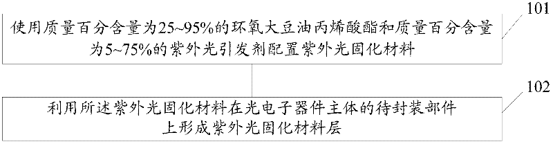
[0076] 202. Configure UV curing materials:

[0077] After mixing the synthes...

Embodiment 2

[0088] Embodiment 2 The encapsulation method of the organic solar cell device and the organic solar cell device after the encapsulation, the organic solar cell device after the encapsulation is as follows Figure 5 shown.

[0089] The encapsulation method includes:

[0090] 301. Synthetic epoxy soybean oil acrylate:

[0091] Add epoxidized soybean oil and polymerization inhibitor p-hydroxyanisole into the reaction vessel in proportion, heat the reaction, add the catalyst triphenylphosphine and acrylic acid at 100°C, and reflect until the acid value of the system drops to 8mgKOH / g, Stop reaction, obtain epoxidized soybean oil acrylate, wherein, the mol ratio of epoxidized soybean oil and acrylic acid is 1.12: 1, catalyst accounts for 1.2% of all reactants gross mass, and polymerization inhibitor accounts for 0.12% of all reactants gross mass .

[0092] 302. Configure UV curing materials:

[0093] The synthesized epoxy soybean oil acrylate is mixed with the active diluent tr...

Embodiment 3

[0104] Embodiment 3 The packaging method of the organic thin film transistor device and the packaged organic thin film transistor device, the packaged organic thin film transistor device is as follows Figure 6 shown.

[0105] The methods include:

[0106] 401. Synthetic epoxy soybean oil acrylate:

[0107] Add epoxidized soybean oil, polymerization inhibitor tris (N-nitroso-N-phenylhydroxylamine) aluminum salt in proportion to the reaction vessel, heat the reaction, add catalyst p-methoxycresol and Acrylic acid, when reflecting until system acid value drops to 8mgKOH / g, stops reaction, obtains epoxidized soybean oil acrylate. Wherein, the molar ratio of epoxidized soybean oil to acrylic acid is 1.2:1, the catalyst accounts for 2% of the total mass of all reactants, and the polymerization inhibitor accounts for 0.5% of the total mass of all reactants.

[0108] 402. Configure UV curing materials:

[0109] After mixing the synthesized epoxy soybean oil acrylate and the react...


PUM


Abstract

The invention discloses a thin-film packaging component, a photoelectronic device and a packaging method of the photoelectronic device and relates to the technical field of photoelectrons. Water and oxygen can be effectively isolated, and the service life of the photoelectronic device can be prolonged. The thin-film packaging component comprises a thin-film packaging layer, wherein the thin-film packaging layer comprises an ultraviolet light curing material layer; the ultraviolet light curing material layer is made from an ultraviolet light curing material; the ultraviolet light curing material comprises 25 to 95 percent of epoxidized soybean oil acrylate and 5 to 75 percent of ultraviolet light initiator. The packaging method disclosed by the invention can be used for packaging the photoelectronic device.

Description

technical field [0001] The invention relates to the technical field of optoelectronics, in particular to a thin film package, an optoelectronic device and a packaging method thereof. Background technique [0002] Optoelectronic technology uses the characteristics of photons and electrons to realize the conversion, transmission and processing of information and energy through a certain medium. It has a wide range of applications and has penetrated into various fields of modern technology and life. The core of optoelectronic technology is optoelectronic devices, which are devices that can convert signals and energy between optoelectronics, electro-optics, and electro-optics. In optoelectronic devices, especially organic electroluminescent devices (OLEDs), the organic functional layers in their components are very sensitive to water, oxygen, etc., and easily react with water or oxygen to form black spots that do not emit light. Encapsulation techniques are therefore required t...

Claims


Application Information

Patent Timeline
Patent Type & Authority Applications(China)
IPC IPC(8): H01L51/52H01L51/56
CPCY02E10/549H10K10/88H10K30/88H10K50/8445H10K50/844
Inventor 陈珉于军胜
Owner BOE TECH GRP CO LTD
Why Eureka
Try Eureka