System and method for machining LED (light-emitting diode) substrate by laser

A laser processing and substrate technology, applied in the direction of laser welding equipment, metal processing equipment, manufacturing tools, etc., can solve the problems of thermal damage, low processing efficiency, high production cost, etc., to reduce production costs, improve production efficiency, and improve light output Effects on Efficiency and Production Yield

Inactive Publication Date: 2012-09-12
HANGZHOU SILAN AZURE
View PDF9 Cites 15 Cited by
  • Summary
  • Abstract
  • Description
  • Claims
  • Application Information

AI Technical Summary

Problems solved by technology

However, an important problem in laser scribing is that the excessively high laser energy at the focal point during the scribing process causes thermal damage, which leads to the diffusion of cracks near the scribing, or the reduction of luminous efficiency caused by thermal melting, etc.
Another problem of laser scribing is the scribing efficiency. From the early 3 pieces / hour to the current mainstream 10 pieces / hour, the speed of scribing efficiency has become the core competitive factor of laser scribing machines.
[0006] To sum up, in the LED substrate processing technology, the thinning and scribing process is an indispensable and interrelated step in the LED chip manufacturing process, but in the traditional process method, the technology used in these two steps The methods are completely different and independent of each other, which will lead to high production costs and low processing efficiency, and there are also problems of low efficiency and low processing quality in their respective process links

Method used


Image

  • System and method for machining LED (light-emitting diode) substrate by laser
  • System and method for machining LED (light-emitting diode) substrate by laser
  • System and method for machining LED (light-emitting diode) substrate by laser

Examples


Embodiment Construction

[0056] The present invention will be further described below in conjunction with specific embodiments and accompanying drawings, but the protection scope of the present invention should not be limited thereby.

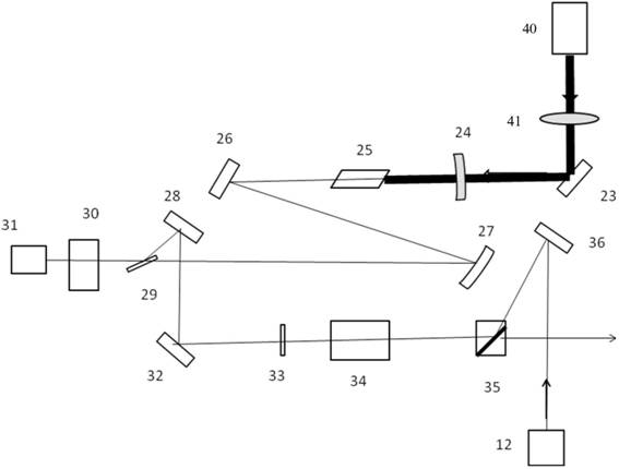
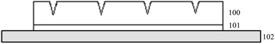
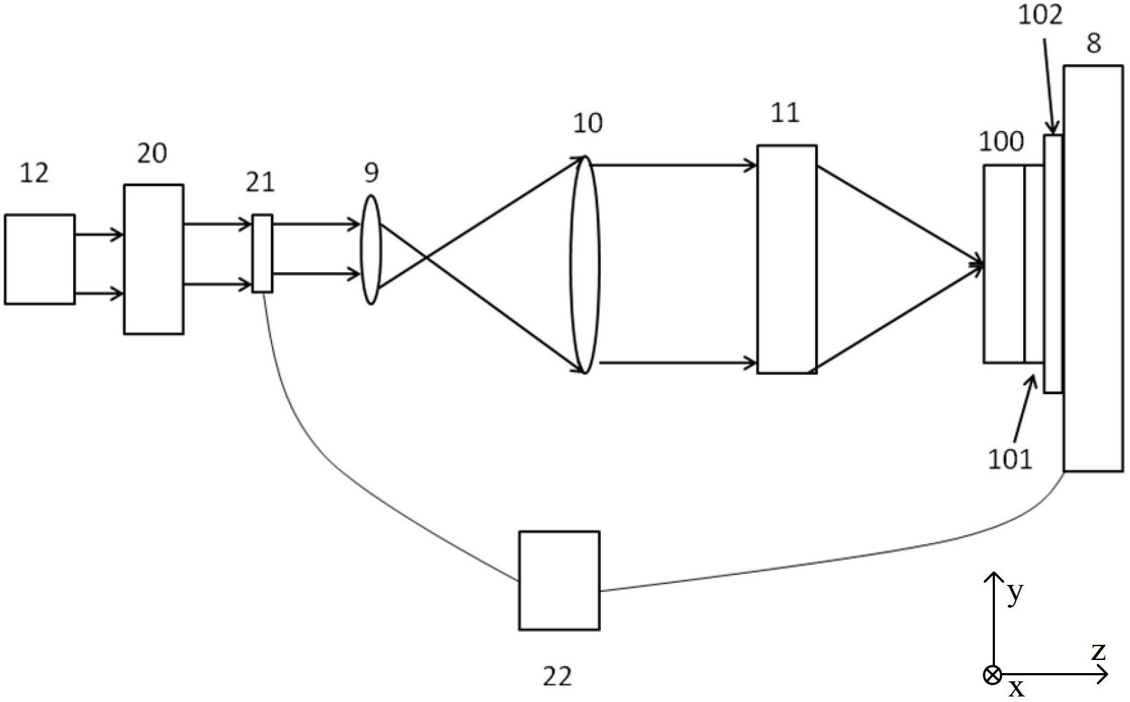
[0057] figure 1 The system for laser processing LED substrates of this embodiment is shown, including: a femtosecond pulse seed laser source 12, a laser amplification beam expansion device (including a laser amplifier 20, an optical gate 21, a beam expansion lens combination device, and a cylindrical lens 11) , the bearing part 8, and the synchronous controller 22.

[0058] Wherein, the femtosecond pulse seed laser source 12 is used to emit femtosecond pulse laser. As a non-limiting example, the femtosecond pulse seed laser source 12 in this embodiment can be realized by a mode-locked fiber femtosecond laser, and the specific parameters are as follows: the pulse width is between 20 ~ 150fs, the center wavelength is 800nm, and the repetition rate is 20~80MHz, the puls...


PUM

PropertyMeasurementUnit
poweraaaaaaaaaa
sizeaaaaaaaaaa
wavelengthaaaaaaaaaa

Abstract

The invention provides a system and method for machining an LED (light-emitting diode) substrate by laser. The system comprises a femtosecond pulse seed laser source, a laser amplifying and beam expanding device and a bearing component, wherein the laser amplifying and beam expanding device carries out energy amplification, beam expansion and line focalization on femtosecond pulse laser given out by the femtosecond pulse seed laser source and outputs a linear light spot; the length of the linear light spot is more than or equal to the diameter of the LED substrate; the bearing component is used for bearing the LED substrate; and the linear light spot is focalized in the LED substrate or on the surface of the LED substrate. By using the system and the method, the LED substrate can be machined by adopting the femtosecond laser; a thinning process and a scribing process are beneficially integrated; the production efficiency is improved; and the production cost is reduced.

Description

technical field [0001] The invention relates to a system and a method for laser processing an LED substrate, in particular to a system and a method for processing an LED substrate by using a femtosecond laser. Background technique [0002] As we all know, the LED wafer is grown on the sapphire or silicon carbide substrate by vapor deposition method based on the light-emitting active layer of gallium nitride-based materials. At present, the size of the common LED wafer is 2 inches to 4 inches. The development of the LED industry, the reduction of LED prices and the improvement of luminous efficiency have driven the popularization of LED chips, which has also driven various technologies used in the LED field. [0003] In the current LED substrate processing process, one of the steps is to reduce the thickness of the LED substrate through physical grinding technology, so as to improve the heat dissipation performance of the LED and increase the light extraction efficiency. How...

Claims


Application Information

Patent Timeline
Patent Type & Authority Applications(China)
IPC IPC(8): B23K26/04B23K26/06B23K26/40B23K26/046B23K26/064B23K26/402
Inventor 高耀辉张昊翔金豫浙封飞飞万远涛李东昇江忠永
Owner HANGZHOU SILAN AZURE
Why Eureka
Try Eureka