Method for cleaning surface of passivated GaAs substrate

A substrate surface, substrate technology, applied in chemical instruments and methods, cleaning methods and utensils, cleaning methods using liquids, etc., can solve the problems of GaAs surface defects, strong irritating taste, environmental hazards, etc. The effect of surface flatness, improved electrical properties, and simple process

Inactive Publication Date: 2012-09-19
NANJING UNIV
View PDF4 Cites 9 Cited by
  • Summary
  • Abstract
  • Description
  • Claims
  • Application Information

AI Technical Summary

Problems solved by technology

However, these cleaning agents currently used are volatile, have a strong pungent taste, or are highly corr

Method used


Image

  • Method for cleaning surface of passivated GaAs substrate
  • Method for cleaning surface of passivated GaAs substrate
  • Method for cleaning surface of passivated GaAs substrate

Examples


Embodiment Construction

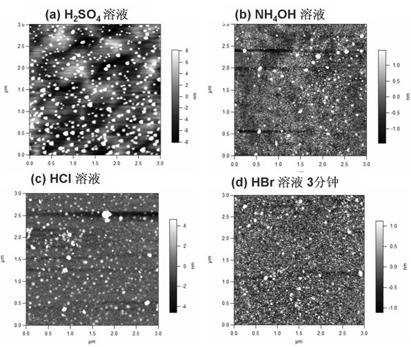
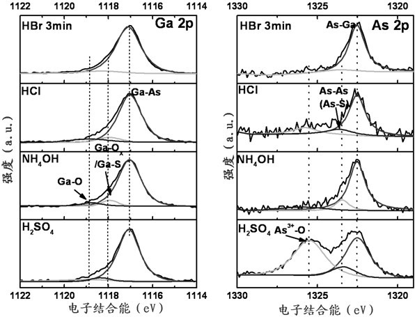
[0016] 1. Cleaning and passivation process of GaAs surface:

[0017] Substrate: Commercial single crystal GaAs substrate, P-type or N-type, orientation (1 0 0), Zn doping concentration is about ~1~10×10 17 cm -3 .

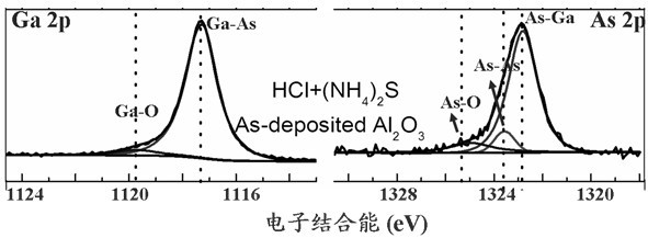
[0018] Process flow: The GaAs substrate is first treated with an organic solution - ultrasonically cleaned with acetone, methanol, and isopropanol for 5 minutes to remove the oil on the surface, then soaked in an acidic or alkaline solution to remove the oxide layer on the surface, and then placed in a heating to 50°C (NH 4 ) 2 Soak in S solution for 20-30 minutes for passivation. Finally, rinse the surface with deionized water and blow dry with high-purity nitrogen.

[0019] Wherein the acidic or alkaline solution that is used to remove oxide layer has following four kinds, and first three kinds of schemes are used for comparing with the fourth kind of scheme of the present invention:

[0020] 1. Soak in a mixed solution with a volume ratio of sulfuric acid...


PUM


Abstract

The invention discloses a method for cleaning the surface of a passivated GaAs substrate. The method comprises the following steps of: treating a GaAs substrate by organic solution to remove oil stain on the surface at first; then soaking the GaAs substrate by hydrobromic acid solution to remove an oxide layer on the surface; then placing the GaAs substrate in (NH4)2S solution which is heated to 50 DEG C and soaking the GaAs substrate for 20-30 minutes to passivate; and finally washing the surface of the passivated GaAs substrate by deionized water and blow-drying the surface by high-purity nitrogen. According to the invention, the green and environment-friendly hydrobromic acid solution is used for cleaning and removing oxides on the surface of the GaAs substrate, and then ammonium sulphide solution is used for passivating the surface of the substrate to effectively enhance the smoothness of the surface and greatly improve the interface quality between a gate dielectric film and the GaAs substrate, thus obviously improving the electric performances of a GaAs-based MOS (metal oxide semiconductor) apparatus. The method is simple in process, and has an important application prospect in preparation for a GaAs-based MOSFET (metal-oxide-semiconductor field-effect transistor) apparatus.

Description

technical field [0001] The invention relates to a process for preparing a CMOS device with a GaAs substrate, in particular to a method for cleaning and passivating the surface of a GaAs substrate during the preparation process. Background technique [0002] As the size of CMOS devices continues to shrink, the improvement of the operating speed of traditional Si-based devices deviates from Moore's law. At present, the research on high dielectric materials in the field of traditional silicon-based integrated circuits has made great progress. The 32nm technology Sandy Bridge processor produced by Intel uses the second generation of high K (0.9nm equivalent oxide thickness high dielectric materials) ), metal grid technology manufacturing, and achieved complete success. with high k The introduction of gate dielectric and metal gate materials, while reducing the high power consumption of small-scale complementary CMOS devices, also brings about the deterioration of the channel ...

Claims


Application Information

Patent Timeline
IPC IPC(8): B08B7/04B08B3/08H01L21/02
Inventor 付盈盈李爱东曹燕强李学飞吴迪
Owner NANJING UNIV
Why Eureka
Try Eureka