Flexible display substrate and preparation method thereof

A flexible display and flexible substrate technology, applied in semiconductor/solid-state device manufacturing, electrical components, electrical solid-state devices, etc., to achieve the effects of reducing costs, improving quality, and fast response speed

Active Publication Date: 2012-09-19
BOE TECH GRP CO LTD
View PDF4 Cites 8 Cited by
  • Summary
  • Abstract
  • Description
  • Claims
  • Application Information

AI Technical Summary

Problems solved by technology

[0007] Therefore, the existing TFT array substrate cannot fully meet the requirements of flexible display devices, and its structure and materials of each layer need to be improved, and materials with good flexibility and strength should be selected to ensure that it is not easy to break when it is bent and used many times. , and improve device performance and yield

Method used


Image

  • Flexible display substrate and preparation method thereof
  • Flexible display substrate and preparation method thereof
  • Flexible display substrate and preparation method thereof

Examples


Embodiment 1

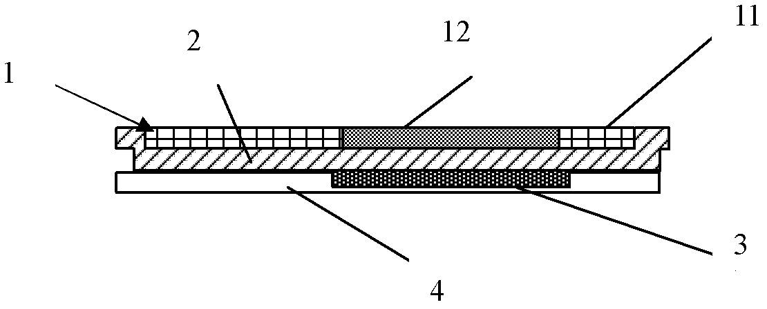
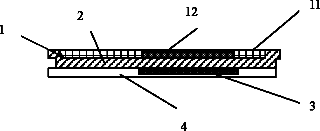
[0054] like figure 1 As shown, the flexible display substrate of the present invention includes a graphene layer 1 , an insulating layer 2 , and a gate electrode 3 in sequence. The graphene layer 1 and the gate electrode 3 are separated by an insulating layer 2, and the gate electrode 3 is covered with a PET film 4. The channel region of the graphene layer 1 is hydrogenated graphene 12, and the rest is intrinsic graphene 11. Intrinsic graphene 11 serves as source, drain and pixel electrodes, and hydrogenated graphene 12 serves as a semiconductor layer.

[0055] The graphene layer 1 is composed of a single-layer graphene layer formed by high temperature chemical vapor deposition.

[0056] The thickness of the PET film 4 is between 30-3000nm, specifically 30nm, 100nm, 500nm, 1000nm and 3000nm.

[0057] The insulating layer 2 is made of PMMA (polymethyl methacrylate), and its thickness is 200 nm.

[0058] The material of the gate electrode 3 is copper, and its thickness is 80 ...

Embodiment 2

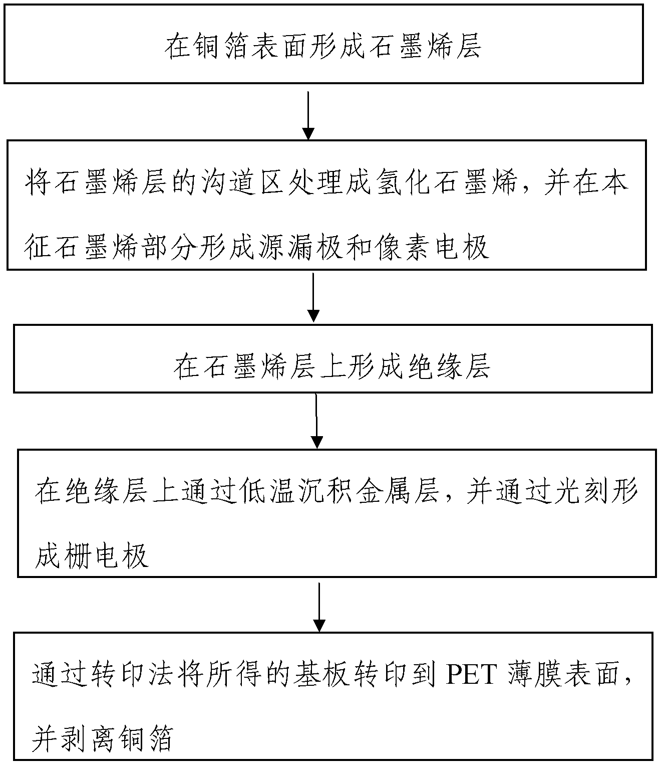
[0066] like figure 2 As shown, the flexible display substrate of this embodiment is prepared according to the following method:

[0067] 1) Form a graphene layer on the surface of the copper foil by high-temperature chemical vapor deposition: place the copper foil in the middle of the quartz tube, put it into an electric furnace, and feed 500 sccm hydrogen into the quartz tube as a carrier gas. After 30 minutes, start heating. When the temperature in the central area of ​​the electric furnace reaches 800°C, methane is introduced into the hydrogen gas as a carbon source for reaction. After the reaction has been carried out for 60 minutes, stop feeding methane, stop heating, cool to room temperature, and deposit a layer of graphene on the surface of the copper foil. , repeated twice to form 3 layers of graphene layer 1 .

[0068] 2) Spin-coat photoresist (Photoresist PR) on the graphene layer 1, etch after exposure and development to expose the graphene layer in the channel re...

Embodiment 3

[0074] like figure 2 As shown, the flexible display substrate of this embodiment is prepared according to the following method:

[0075] 1) Form a graphene layer on the surface of the copper foil by high-temperature chemical vapor deposition: place the copper foil in the middle of the quartz tube, put it into an electric furnace, and feed 100 sccm hydrogen and 200 sccm argon into the quartz tube as the carrier gas. After 10 minutes, , start heating, when the temperature in the central area of ​​the electric furnace reaches 1500°C, feed methane into hydrogen and argon as a carbon source for reaction, after 60 minutes of reaction, stop feeding methane, stop heating, cool to room temperature, A layer of graphene is deposited on the surface of the foil, and repeated several times to form 10 graphene layers 1 .

[0076] 2) Spin-coat the photoresist (Photoresist PR) on the graphene layer 1, etch after the mask to expose the graphene channel region, and use the electron cyclotron r...


PUM

PropertyMeasurementUnit
Thicknessaaaaaaaaaa
Thicknessaaaaaaaaaa

Abstract

The invention provides a substrate and a preparation method thereof. The substrate comprises a flexible substrate, a graphene layer (1), an insulating layer (2) and a gate electrode (3), wherein the graphene layer (1) is separated from the gate electrode (3) by the insulating layer (2); the gate electrode (3) is arranged on the flexible substrate; and the graphene layer (1) comprises a source electrode and a drain electrode of a intrinsic (11) material and a semiconductor layer which is positioned between the source electrode and the drain electrode and is made of a graphene hydroxide (12) material. The flexible display substrate is formed on a metal thin film and then adhered to the flexible substrate, so that the formed flexible display substrate has higher flatness and mass, the performance and the yield of the device can be improved excellently, and occurrence of poor pixel is not easily caused after multiple bending.

Description

technical field [0001] The present invention relates to a flexible display substrate, in particular to a flexible display substrate and a preparation method thereof. Background technique [0002] As a new type of display device that replaces rigid displays, flexible displays have attracted more and more attention, and are widely used in e-books, paper in books and magazines, point-of-sale (POS) terminal equipment, indoor and outdoor signs, smart cards and In products such as retail shelf labels. [0003] At present, the basic structure of the TFT array substrate is: sequentially form the gate (metal) on the glass, the gate insulating layer (SiO 2 , SiNx, resin layer, etc.), semiconductor layer (amorphous silicon, polycrystalline silicon, microcrystalline silicon), contact layer (N+ layer), source and drain layer (metal), followed by pixel electrode (ITO). [0004] However, when it is used as a flexible display, the amorphous silicon and other materials of the semiconductor...

Claims


Application Information

Patent Timeline
IPC IPC(8): H01L29/16H01L27/12H01L21/77
Inventor 戴天明薛建设姚琪张峰
Owner BOE TECH GRP CO LTD
Why Eureka
Try Eureka