Nonmagnetic Ru film and production method thereof
A non-magnetic, thin-film technology, applied in the field of information storage, can solve the problem that the surface morphology of thin-film Ru film is not clearly stated
- Summary
- Abstract
- Description
- Claims
- Application Information
AI Technical Summary
Problems solved by technology
Method used
Image
Examples
preparation example Construction
[0019] Described ruthenium film adopts the method for magnetron sputtering to make, and concrete preparation method comprises the following steps:
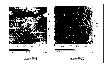
[0020] (1) Treatment of the substrate material: the (111) surface of the silicon single wafer is used as the substrate surface, and after alternating ultrasonic cleaning with acetone and ethanol, it is cleaned with ion beam pre-sputtering to remove impurities on the surface of the Si wafer. In ion beam pre-sputter cleaning, the background vacuum is better than 10 -4 Pa, the working pressure of inert gas during sputtering is 1x10 -2 Pa to 4x10 -2 Pa.
[0021] (2) Magnetron sputtering coating: Put the cleaned Si wafer into the magnetron sputtering equipment, and use a self-made Ru target for coating. Sputtering was performed at room temperature with a background vacuum of 10 -3 ~10 -4 Pa, the working pressure of Ar gas is 0.5~3Pa, the sputtering power is 50~300W, and the self-bias voltage is 100~600V.
Embodiment 1
[0024] The ruthenium thin film of the present invention is made through the following steps:
[0025] (1) Treatment of the substrate material: the (111) surface of the silicon single wafer is used as the substrate surface, and after alternating ultrasonic cleaning with acetone and ethanol, it is cleaned with ion beam pre-sputtering to remove impurities on the surface of the Si wafer. Ion beam pre-sputter cleaning with a background vacuum of 6x10 -4 Pa, the working pressure of inert gas during sputtering is 2x10 -2 Pa.
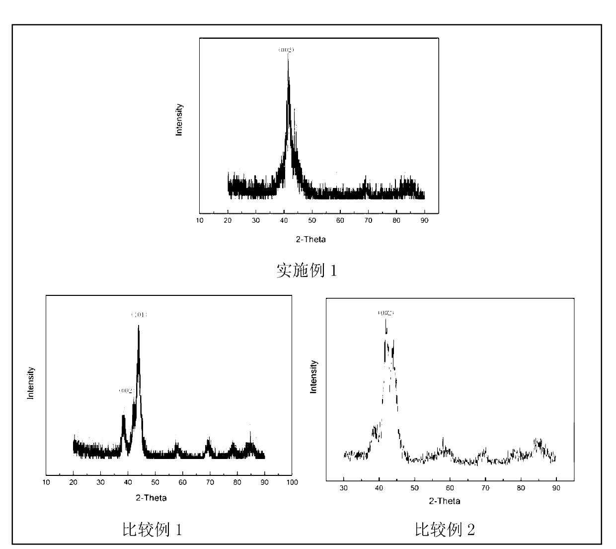
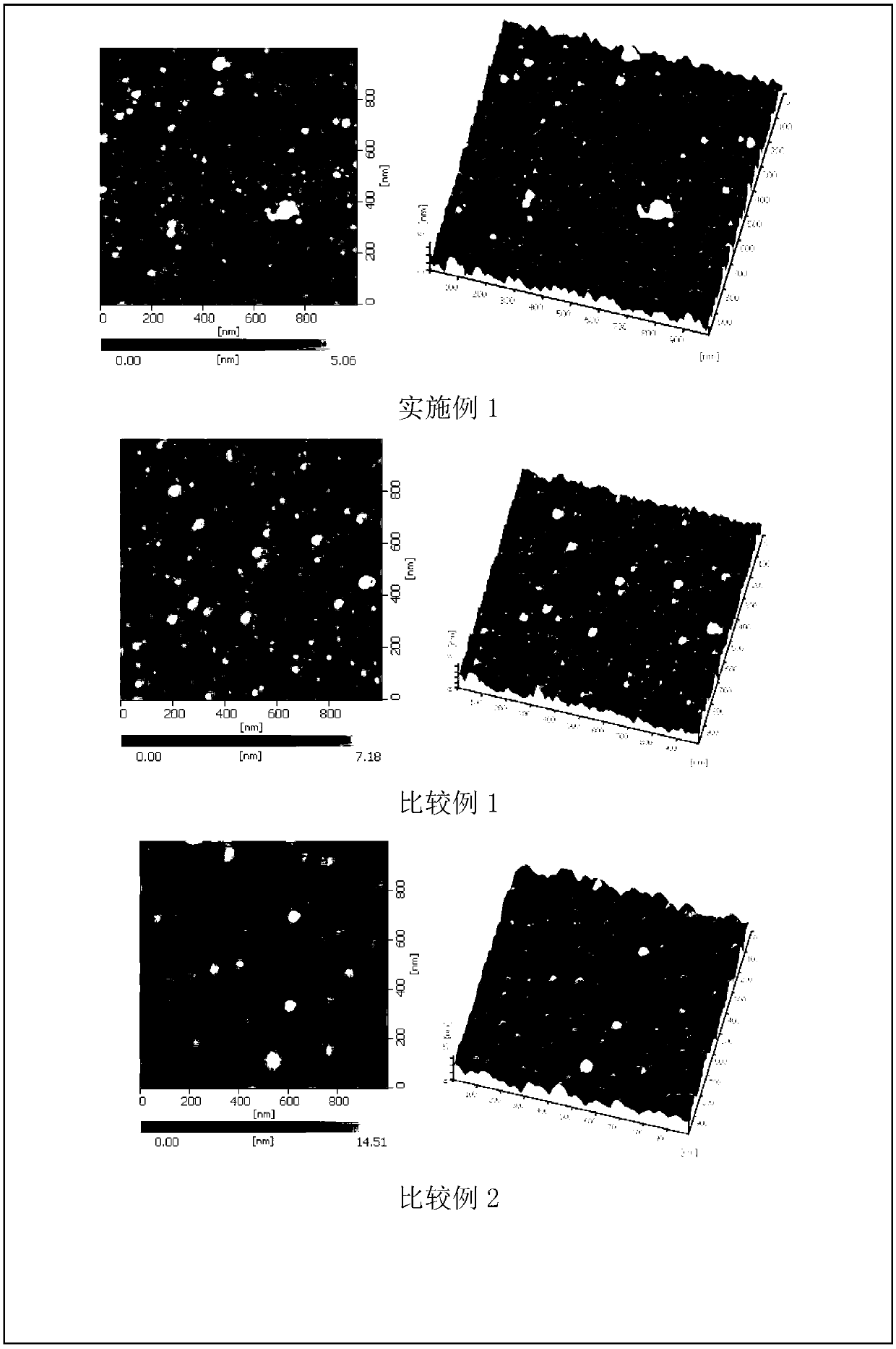
[0026] (2) Magnetron sputtering coating: Put the cleaned Si wafer into the magnetron sputtering equipment, and use a self-made ruthenium target (1#) for coating. The average grain size of the ruthenium target (1#) is 4.3 μm. In the X-ray diffraction analysis, the X-ray diffraction peak intensity ratio of the (002) crystal plane represented by the formula (1) was 42.1%. Sputtering was performed at room temperature with a background vacuum of 3x10 -3 Pa, th...
Embodiment 2
[0028] The difference from Example 1 lies in that during the magnetron sputtering coating process, the working pressure of Ar gas is 0.5Pa, the sputtering power is 300W, and the self-bias voltage is 600V.
PUM
| Property | Measurement | Unit |
|---|---|---|
| size | aaaaa | aaaaa |
| surface roughness | aaaaa | aaaaa |
| surface roughness | aaaaa | aaaaa |
Abstract
Description
Claims
Application Information


