Method for preparing double-faced back contact solar cell

A solar cell and back contact technology, applied in the field of solar cells, can solve problems such as complicated process, damage to non-expanded boron suede surface, complicated operation, etc., and achieve the effects of simple preparation process, improved quality, and simplified process flow

Active Publication Date: 2012-10-03
CSI CELLS CO LTD +1
View PDF7 Cites 7 Cited by
  • Summary
  • Abstract
  • Description
  • Claims
  • Application Information

AI Technical Summary

Problems solved by technology

Obviously, this step is complicated to operate, and may cause damage to the suede surface of the non-bored surface
In addition, the secondary diffusion process also makes the whole process more complicated

Method used


Image

  • Method for preparing double-faced back contact solar cell
  • Method for preparing double-faced back contact solar cell
  • Method for preparing double-faced back contact solar cell

Examples


Embodiment 1

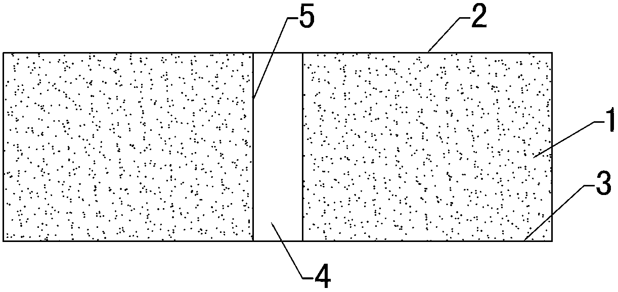
[0051] see Figure 1~9 Shown, a kind of preparation method of double-sided back-contact solar cell comprises the steps:

[0052] (1) Open a hole on the N-type silicon chip 1, and the hole wall 5 of the hole 4 is as figure 1 shown;

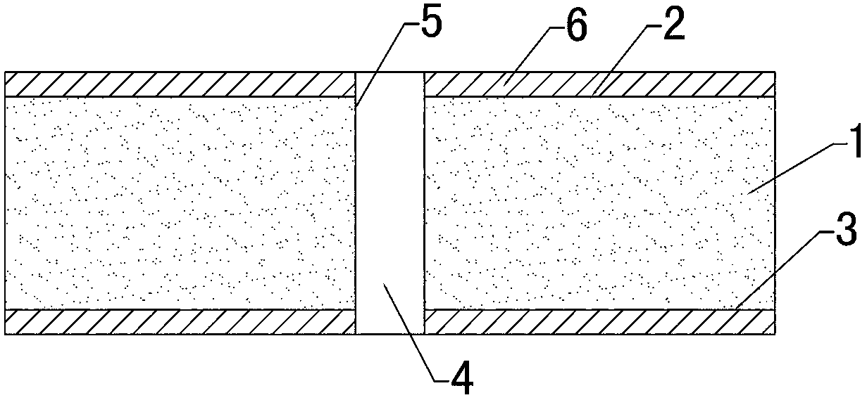
[0053] (2) Clean the surface of the silicon chip, remove the damaged layer, and carry out texturing on the front side 2 and the back side 3 of the silicon chip to form a textured surface 6, such as figure 2 shown;

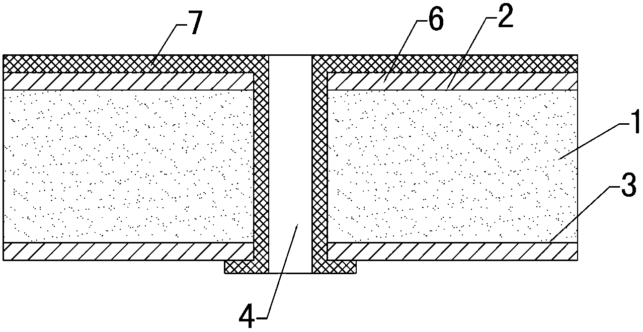
[0054] (3) Print boron paste 7 on the front side of the silicon wafer and in the holes, the mass concentration of boric acid in the boron paste is 20%, and dry at 250°C for 2 minutes; print boron paste on the area around the hole on the back of the silicon wafer, and dry at 250°C 2 minutes, such as image 3 ;

[0055] (4) Phosphorus paste 8 is printed on the non-peripheral area of ​​the backside of the silicon wafer, the mass concentration of phosphoric acid in the phosphorous paste is 25%, and it is dried at 250°C for 2 minutes, ...

Embodiment 2

[0063] see Figure 10~18 Shown, a kind of preparation method of double-sided back-contact solar cell comprises the steps:

[0064] (1) Clean the surface of the N-type silicon chip 1, remove the damaged layer, and make texture on the front side 2 and the back side 3 of the silicon chip to form a textured surface 6, such as Figure 10 ;

[0065] (2) Print boron paste 7 on the front side of the silicon wafer, the mass concentration of boric acid in the boron paste is 20%, and dry at 250°C for 2 minutes, as Figure 11 ;

[0066] (3) Phosphate paste 8 is printed on the non-hole area on the back of the silicon wafer, the mass concentration of phosphoric acid in the phosphor paste is 30%, and it is dried at 250°C for 2 minutes, as Figure 12 ;

[0067] (4) PECVD is used to deposit a silicon oxide barrier layer 9 on the front and back sides of the silicon wafer, and its thickness is 90nm, such as Figure 13 ;

[0068] (5) Anneal the silicon wafer obtained in step (4) at 900°C to...

Embodiment 3

[0074] A method for preparing a double-sided back-contact solar cell, comprising the steps of:

[0075] (1) Open holes on the P-type silicon wafer;

[0076] (2) Clean the surface of the silicon wafer, remove the damaged layer, and make texture on the front and back of the silicon wafer to form a textured surface;

[0077] (3) Print phosphorous slurry on the front side of the silicon wafer and in the holes, the mass concentration of phosphoric acid in the phosphoric acid slurry is 15%, and dry at 250°C for 2 minutes; print phosphorous paste on the area around the hole on the back of the silicon wafer, and dry at 250°C for 2 minutes minute;

[0078] (4) Print boron paste on the non-peripheral area of ​​the backside of the silicon wafer, the mass concentration of boric acid in the boron paste is 30%, and dry at 250°C for 2 minutes;

[0079] (5) PECVD is used to deposit a silicon oxide barrier layer on the front and back sides of the silicon wafer, with a thickness of 90nm;

[...


PUM


Abstract

The invention discloses a method for preparing a double-faced back contact solar cell, comprising following steps: (1) holing; (2) washing, and texturizing the front face and the back face of a silicon wafer; (3) arranging a first doping agent on the front face and in the hole of the silicon wafer, and arranging the first doping agent in the surrounding area of the hole in the back face of the silicon wafer, wherein the doping type of the first doping agent is opposite to that of the silicon wafer; (4) arranging a second doping agent in the non-hole surrounding area on the back face of the silicon wafer, wherein the doping type of the second doping agent is the same as that of the silicon wafer; (5) growing barrier layers on the front face and the back face of the silicon wafer; (6) annealing the silicon wafer at the temperature of 800 to 1000 DEG C, diffusing and making junctions; (7) etching peripheral junctions; (8) washing and removing the barrier layers; (9) arranging passivation anti-reflection films on the front face and the back face of the silicon wafer; and (10) arranging a porous metal electrode in the hole, printing and sintering. Adopting a method for arranging the doping agents, i.e. adopting the various type doping agents on two faces of the silicon wafer, the double-faced back contact solar cell realizes the co-diffusion of boron-phosphor in the presence of the barrier layers, thereby greatly simplifying process flows and reducing the production cost.

Description

technical field [0001] The invention relates to a preparation method of a double-sided back-contact solar cell, which belongs to the field of solar cells. Background technique [0002] Conventional fossil fuels are being exhausted day by day. Among the existing sustainable energy sources, solar energy is undoubtedly the cleanest, most common and most potential alternative energy source. At present, among all solar cells, crystalline silicon solar cells are one of the solar cells that have been widely commercialized. This is due to the extremely abundant reserves of silicon materials in the earth's crust. , has excellent electrical and mechanical properties. Therefore, crystalline silicon solar cells occupy an important position in the field of photovoltaics. High efficiency is the current development trend of crystalline silicon solar cells. The conversion efficiency of solar cells is improved by improving surface texture, selective emission junction, passivation of the fr...

Claims


Application Information

Patent Timeline
Patent Type & Authority Applications(China)
IPC IPC(8): H01L31/18
CPCY02P70/50
Inventor 王栩生章灵军
Owner CSI CELLS CO LTD
Why Eureka
Try Eureka