Isolated gate field effect transistor and manufacture method thereof

A technology of field effect transistors and manufacturing methods, applied in the field of microelectronics, can solve the problems of threshold voltage drift, dielectric layer thickness cannot be accurately controlled, etc., and achieve the effects of improving structural quality, suppressing current collapse effect, and avoiding air pollution

Active Publication Date: 2012-10-10
昆山工研院第三代半导体研究院有限公司
View PDF3 Cites 17 Cited by
  • Summary
  • Abstract
  • Description
  • Claims
  • Application Information

AI Technical Summary

Problems solved by technology

However, due to the repeatability of the etching process, the thickness of the remaining di

Method used


Image

  • Isolated gate field effect transistor and manufacture method thereof
  • Isolated gate field effect transistor and manufacture method thereof
  • Isolated gate field effect transistor and manufacture method thereof

Examples


Embodiment Construction

[0047] The present invention will be described in detail below in conjunction with specific embodiments shown in the accompanying drawings. However, these embodiments do not limit the present invention, and any structural, method, or functional changes made by those skilled in the art according to these embodiments are included in the protection scope of the present invention.

[0048] Furthermore, repeated reference numerals or designations may be used in different embodiments. These repetitions are only for the purpose of simply and clearly describing the present invention, and do not represent any relationship between the different embodiments and / or structures discussed.

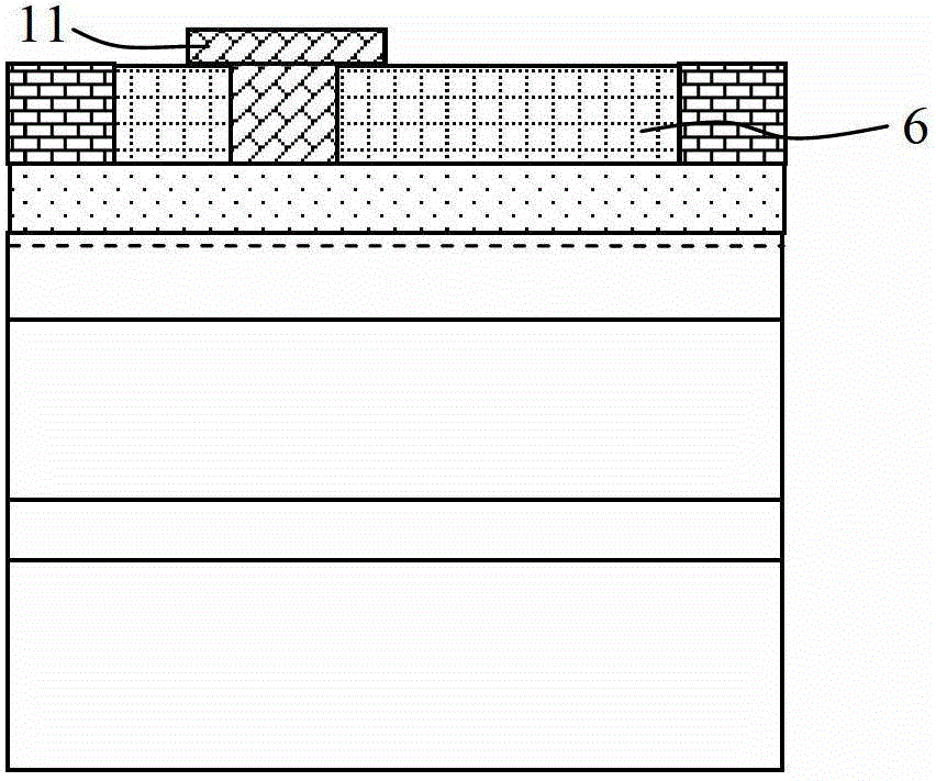
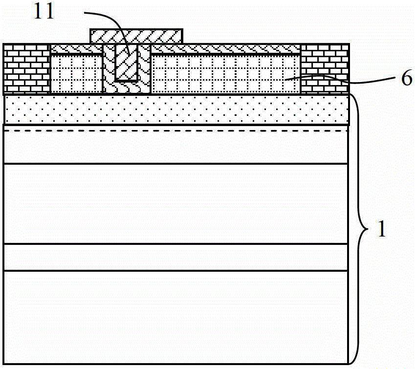
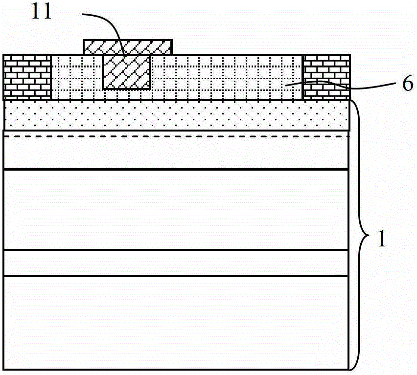
[0049] ginseng Figure 2e As shown, in the first embodiment of the present invention, the insulated gate field effect transistor includes: a substrate 1 and a nitride nucleation layer 2, a nitride buffer layer 3, a nitride channel layer 4, Nitride barrier layer 5, silicon nitride layer 6 (first dielect...


PUM

PropertyMeasurementUnit
Thicknessaaaaaaaaaa
Thicknessaaaaaaaaaa

Abstract

The invention discloses an isolated gate field effect transistor and the manufacture method thereof. Through the method of introducing metal when a dielectric layer is grown on a nitride transistor structure, the chemical properties of the dielectric layer are changed, and the effects of controlling etching speed and depth can be played. A groove structure is formed in a grid region in a partially thinned manner, and part of dielectric layer is reserved at the grid. A metal grid is arranged on the dielectric layer in the groove region of the grid, so as to form metal/ dielectric layer/ semi-conductor contact, and meanwhile, the groove is used for forming a field plate structure. Since the surface of a semi-conductor is protected by the dielectric layer during the entire technological process, damages to the surface of nitride, stress releasing and staining on the surface of the nitride can be greatly reduced, and the current collapsing effect of a device can be reduced greatly. Due to the MISFET (Metal Insulation Semiconductor Field Effect Transistor) or MOSFET (Metal-Oxide -Semiconductor Field Effect Transistor) structure is formed by the high-quality dielectric layer, current leakage of the grid can be reduced greatly.

Description

technical field [0001] The invention belongs to the technical field of microelectronics, and in particular relates to an insulated gate field effect transistor and a method for manufacturing the insulated gate field effect transistor. Background technique [0002] Group III nitride semiconductors have the characteristics of wide band gap, high dielectric breakdown electric field and high electron saturation drift velocity, and are suitable for making high-temperature, high-speed switching and high-power electronic devices. In GaN-based field-effect transistors, a large amount of charge is generated in the channel layer by piezoelectric polarization and spontaneous polarization. Since the source of the two-dimensional electron gas is the ionization of the donor surface state on the nitride surface, the current density of the nitride transistor is extremely sensitive to the surface state, which is likely to cause the current collapse effect. In addition, during the epitaxial ...

Claims


Application Information

Patent Timeline
IPC IPC(8): H01L29/423H01L29/78H01L21/28H01L21/336
CPCH01L21/28H01L29/78H01L29/423H01L29/7787H01L21/0223H01L21/31111H01L21/31116H01L29/2003H01L29/201H01L29/205H01L29/402H01L29/42364H01L29/513H01L29/517H01L29/518H01L29/66462H01L29/7783H01L29/7786
Inventor 程凯
Owner 昆山工研院第三代半导体研究院有限公司
Why Eureka
Try Eureka