

Dual polycrystalline strain SiGe plane bipolar complementary metal oxide semiconductor (BiCMOS) integrated device and preparation method
An integrated device and double polycrystalline technology, which is applied in semiconductor/solid-state device manufacturing, electric solid-state devices, semiconductor devices, etc., can solve the problems of reducing the precision of lithography, unsatisfactory lithography technology, and difficulty in meeting design.
- Summary
- Abstract
- Description
- Claims
- Application Information
AI Technical Summary
Problems solved by technology
Method used
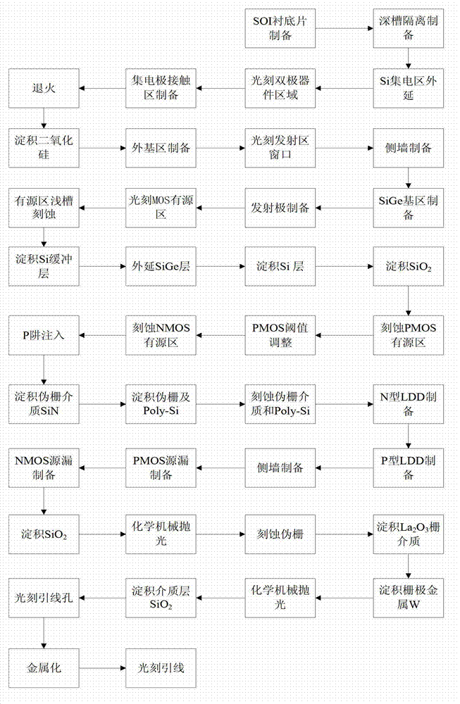
Image

Examples
Embodiment 1
[0120] Embodiment 1: Preparation of dual polycrystalline strained SiGe planar BiCMOS integrated devices and circuits with a channel length of 22 nm, the specific steps are as follows:
[0121] Step 1, SOI substrate material preparation.
[0122] (1a) Select N-type doping concentration as 1×10 15 cm -3 The surface of the Si wafer is oxidized, and the thickness of the oxide layer is 1 μm, which is used as the base material of the upper layer, and hydrogen is injected into the base material;
[0123] (1b) Select the N-type doping concentration as 1×10 15 cm -3 The surface of the Si wafer is oxidized, and the thickness of the oxide layer is 1 μm, which is used as the base material of the lower layer;
[0124] (1c) Use chemical mechanical polishing (CMP) process to polish the surface of the lower layer and the upper layer of the base material after hydrogen injection;
[0125] (1d) Place the polished lower layer and upper layer of the base material surface oxide layer relatively closely, and...
Embodiment 2
[0186] Embodiment 2: Preparation of a dual polycrystalline strained SiGe planar BiCMOS integrated device and circuit with a channel length of 130 nm, the specific steps are as follows:
[0187] Step 1, SOI substrate material preparation.
[0188] (1a) Select the N-type doping concentration to be 3×10 15 cm -3 The surface of the Si wafer is oxidized, and the thickness of the oxide layer is 0.7μm, which is used as the base material of the upper layer, and hydrogen is injected into the base material;
[0189] (1b) Choose N-type doping concentration as 3×10 15 cm -3 The surface of the Si wafer is oxidized, and the thickness of the oxide layer is 0.7μm, as the base material of the lower layer;
[0190] (1c) Use chemical mechanical polishing (CMP) process to polish the surface of the lower layer and the upper layer of the base material after hydrogen injection;
[0191] (1d) Place the polished lower layer and upper layer of the substrate material surface oxide layer relatively close, and plac...
Embodiment 3
[0252] Embodiment 3: Preparation of a dual polycrystalline strained SiGe planar BiCMOS integrated device and circuit with a channel length of 350 nm, the specific steps are as follows:
[0253] Step 1, SOI substrate material preparation.
[0254] (1a) Choose N-type doping concentration as 5×10 15 cm -3 The surface of the Si wafer is oxidized, and the thickness of the oxide layer is 0.5μm, which is used as the base material of the upper layer, and hydrogen is injected into the base material;
[0255] (1b) Select N-type doping concentration as 5×10 15 cm -3 The surface of the Si wafer is oxidized, and the thickness of the oxide layer is 0.5μm, as the base material of the lower layer;
[0256] (1c) Use chemical mechanical polishing (CMP) process to polish the surface of the lower layer and the upper active layer matrix material after hydrogen injection;
[0257] (1d) Place the polished lower layer and upper layer of the substrate material surface oxide layer relatively closely, and place i...
PUM
| Property | Measurement | Unit |
|---|---|---|
| Thickness | aaaaa | aaaaa |
| Thickness | aaaaa | aaaaa |
| Thickness | aaaaa | aaaaa |
Abstract
Description
Claims
Application Information