Plane strain BiCMOS (Bipolar-Complementary Metal-Oxide-Semiconductor) integrated component based on self-aligned technology and preparation method thereof

A self-alignment process and integrated device technology, applied in semiconductor/solid-state device manufacturing, electric solid-state devices, semiconductor devices, etc., can solve high cost, difficulty in preparing large-diameter single crystals, and low mobility of Si material carriers and other issues to achieve the effect of improving performance

Inactive Publication Date: 2012-10-17
XIDIAN UNIV
View PDF3 Cites 0 Cited by
  • Summary
  • Abstract
  • Description
  • Claims
  • Application Information

AI Technical Summary

Problems solved by technology

Although GaAs and InP-based compound devices have superior frequency characteristics, their preparation process is more complicated than Si process, high cost, difficult to prepare large-diameter single crystal, low mechanical strength, poor heat dissipation performance, incompatibility with Si process and lack of SiO 2 Such passivation layer and other factors limit its wide application and development.
[0007] Due to the low mobility of Si mate...

Method used


Image

  • Plane strain BiCMOS (Bipolar-Complementary Metal-Oxide-Semiconductor) integrated component based on self-aligned technology and preparation method thereof

Examples


Embodiment 1

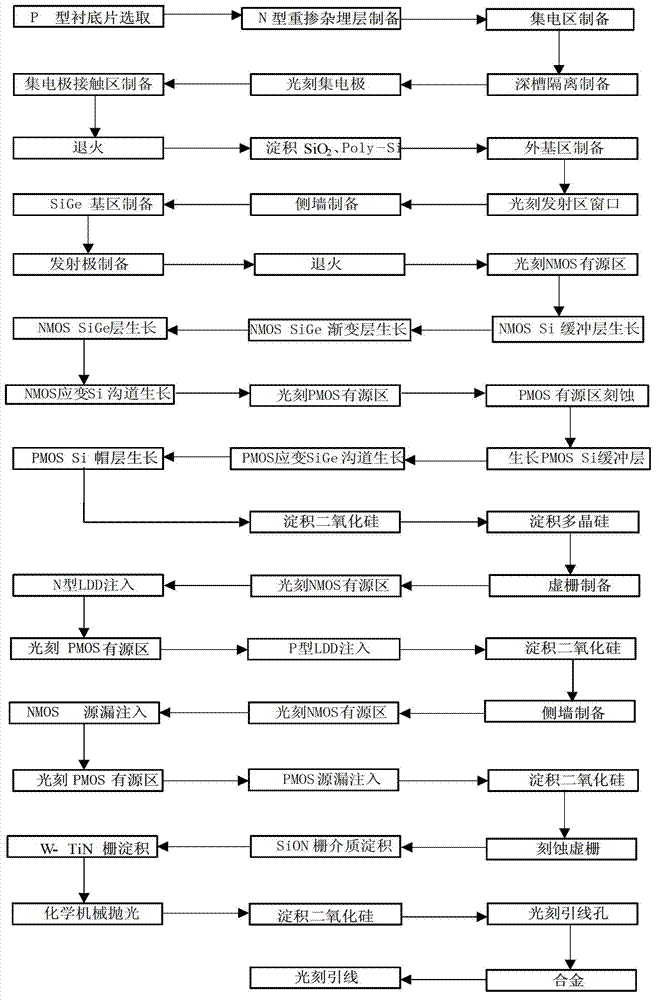
[0124] Embodiment 1: Prepare a strained BiCMOS integrated device and circuit based on a self-alignment process with a conductive channel of 45nm, and the specific steps are as follows:

[0125] Step 1, preparation of the buried layer.

[0126] (1a) Select the doping concentration to be 5×10 14 cm -3 A P-type Si sheet as a substrate;

[0127] (1b) Thermally oxidize a layer of SiO with a thickness of 300nm on the substrate surface 2 layer;

[0128] (1c) Photoetching the buried layer region, implanting N-type impurities into the buried layer region, and annealing at 800° C. for 90 minutes to activate the impurities to form an N-type heavily doped buried layer region.

[0129] Step 2, deep trench isolation preparation.

[0130] (2a) Remove the redundant oxide layer on the surface, and epitaxially grow an N-type epitaxial Si layer with a thickness of 1.5 μm as the collector region, and the doping concentration of this layer is 1×10 16 cm -3 ;

[0131] (2b) Deposit a layer o...

Embodiment 2

[0191] Embodiment 2: The plane-strained BiCMOS integrated device and circuit based on the self-alignment process are prepared with a conductive channel of 30nm, and the specific steps are as follows:

[0192] Step 1, preparation of the buried layer.

[0193] (1a) Select the doping concentration as 1×10 15 cm -3 A P-type Si sheet as a substrate;

[0194] (1b) Thermally oxidize a layer of SiO with a thickness of 400nm on the substrate surface 2 layer;

[0195] (1c) Photoetching the buried layer region, implanting N-type impurities into the buried layer region, and annealing at 900° C. for 60 minutes to activate the impurities to form an N-type heavily doped buried layer region.

[0196] Step 2, deep trench isolation preparation.

[0197] (2a) Remove the excess oxide layer on the surface, and epitaxially grow an N-type epitaxial Si layer with a thickness of 1.8 μm as the collector region, and the doping concentration of this layer is 5×10 16 cm -3 ;

[0198] (2b) Deposit ...

Embodiment 3

[0258] Embodiment 3: Prepare the strained BiCMOS integrated device and circuit based on the self-alignment process with a conductive channel of 22nm, the specific steps are as follows:

[0259] Step 1, preparation of the buried layer.

[0260] (1a) Select the doping concentration to be 5×10 15 cm -3 A P-type Si sheet as a substrate;

[0261] (1b) Thermally oxidize a layer of SiO with a thickness of 500nm on the surface of the substrate 2 layer;

[0262] (1c) Photoetching the buried layer region, implanting N-type impurities into the buried layer region, and annealing at 950° C. for 30 minutes to activate the impurities to form an N-type heavily doped buried layer region.

[0263] Step 2, deep trench isolation preparation.

[0264] (2a) Remove the excess oxide layer on the surface, and epitaxially grow an N-type epitaxial Si layer with a thickness of 2 μm, as the collector region, and the doping concentration of this layer is 1×10 17 cm -3 ;

[0265] (2b) Deposit a laye...


PUM

PropertyMeasurementUnit
Thicknessaaaaaaaaaa
Thicknessaaaaaaaaaa
Thicknessaaaaaaaaaa

Abstract

The invention discloses a plane strain BiCMOS (Bipolar-Complementary Metal-Oxide-Semiconductor) integrated device based on a self-aligned technology and a preparation method thereof. The preparation method comprises the following steps: firstly preparing a buried layer on a substrate slice, growing N-type Si epitaxy, preparing a trench isolation and collector contact region, etching a base region window by using a wet method, selectively growing a SiGe base region, depositing N-type Poly-Si and removing Poly-Si outside an emitter, thus forming a SiGe HBT device; etching active region trenches of an NMOS (Negative-channel Metal Oxide Semiconductor) and a PMOS (Positive-channel Metal Oxide Semiconductor) devices; in the trenches, respectively carrying out selective epitaxial growth of a P-type Si layer, a P-type SiGe graded layer and a P-type SiGe layer serving as the active region of the NMOS device, as well as an N-type Si layer, an N-type strained SiGe layer and an N-type Si cap layer serving as the active region of the PMOS device; preparing a virtual grid and a side wall to form the source drains of the NMOS and the PMOS devices in a self-aligned manner; and preparing a grid to form a CMOS (Complementary Metal-Oxide-Semiconductor) structure so as to finally prepare a strain BiCMOS integrated device and a circuit. According to the method, tension strain Si with high electron mobility and compression strain with high hole mobility are respectively used as the conducting channels of the NMOS and the PMOS devices, thereby efficiently improving the performance of BiCMOS integrated circuit.

Description

technical field [0001] The invention belongs to the technical field of semiconductor integrated circuits, in particular to a plane strain BiCMOS integrated device based on a self-alignment process and a preparation method. Background technique [0002] The integrated circuit, which appeared in 1958, is one of the most influential inventions of the 20th century. Microelectronics, which was born based on this invention, has become the basis of existing modern technology, accelerating the process of knowledge and informationization of human society, and at the same time changing the way of thinking of human beings. It not only provides humans with a powerful tool to transform nature, but also opens up a broad space for development. [0003] Semiconductor integrated circuits have become the basis of the electronics industry, and people's huge demand for the electronics industry has prompted the rapid development of this field. In the past few decades, the rapid development of ...

Claims


Application Information

Patent Timeline
IPC IPC(8): H01L27/06H01L21/8249H01L21/28
Inventor 胡辉勇宋建军宣荣喜舒斌张鹤鸣周春宇戴显英郝跃
Owner XIDIAN UNIV
Why Eureka
Try Eureka