MOSFET pair with stack capacitor and manufacturing method thereof

An oxide semiconductor and field effect transistor technology, which is applied in the field of metal oxide semiconductor field effect transistor pairs and their manufacturing, can solve the problems of high internal resistance and low heat dissipation capacity, and achieves high adaptability, good heat dissipation capacity, and easy use. Effect

Active Publication Date: 2012-10-24
CYNTEC
View PDF2 Cites 11 Cited by
  • Summary
  • Abstract
  • Description
  • Claims
  • Application Information

AI Technical Summary

Problems solved by technology

[0010] According to the above problems, the object of the present invention is to provide a structure with a pair of metal oxide semiconductor field effect transistors and an input capacitor stacked on an upper lead frame to solve the high internal impedance and low heat dissipation capacity of the traditional voltage regulation module The problem

Method used


Image

  • MOSFET pair with stack capacitor and manufacturing method thereof
  • MOSFET pair with stack capacitor and manufacturing method thereof
  • MOSFET pair with stack capacitor and manufacturing method thereof

Examples


Embodiment Construction

[0073] The above and other technical features and advantages of the present invention will be described in more detail below in conjunction with the accompanying drawings.

[0074] The manufacture and use of the preferred embodiments of the present invention are discussed in detail below. However, according to the concept of the present invention, it can include or be applied to a wider range of technologies. It should be noted that the embodiments are only used to disclose the manufacture and use of the present invention. The specific method is not intended to limit the present invention.

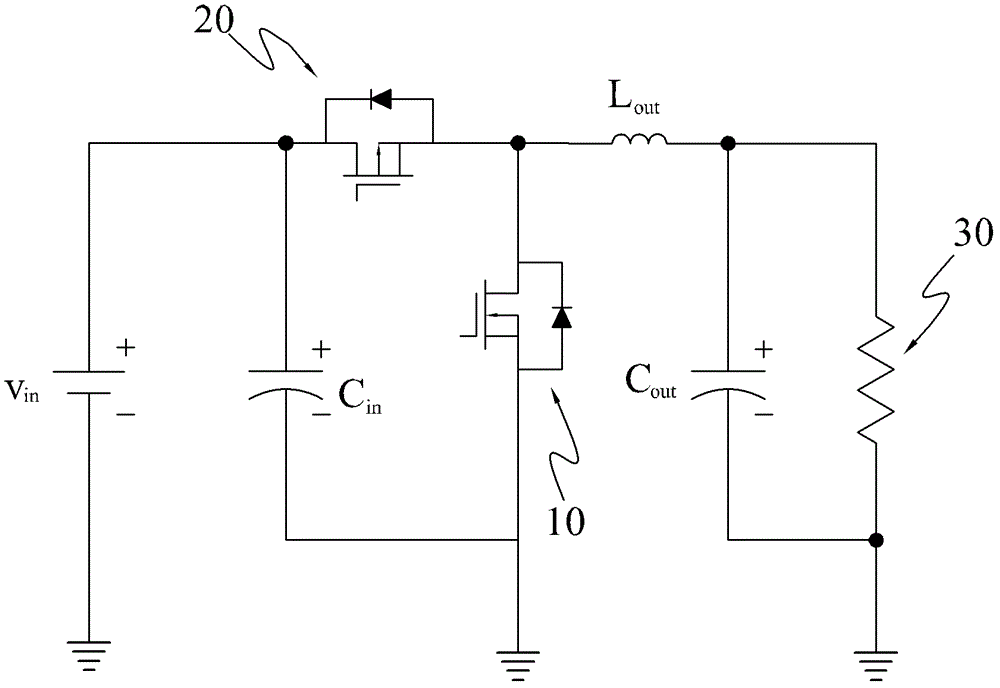
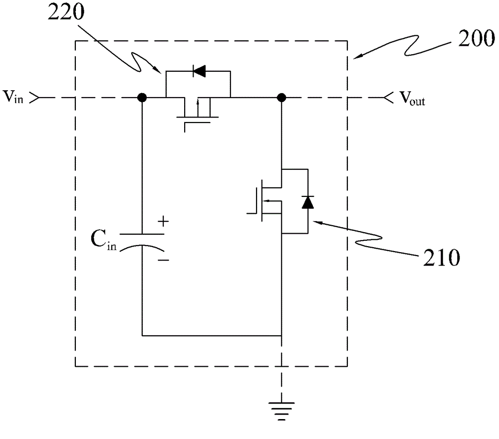
[0075] First, see image 3 , which is a schematic diagram of a circuit diagram of the present invention, showing that a metal oxide semiconductor field effect transistor pair 200 with a stack capacitance includes a first metal oxide semiconductor field effect transistor 210, a second metal oxide semiconductor field effect transistor 220 and A capacitor Cin. The mosfet pair 200 with stack...


PUM


Abstract

A MOSFET pair with a stack capacitor is disclosed herein. It can regulate the input voltage and optimize a short EMI loop. It has a bottom lead frame and an up lead frame, which can simultaneously dissipate the heat generated by two MOSFETs to achieve excellent thermal-dissipation. It can adopt solder, Ag epoxy, or gold balls to implement the electrical bonding of two MOSFETs with the bottom lead frame and the up lead frame to achieve excellent structural flexibility. A device, such as an IGBT, a diode, an inductor, a choke, and a heat sink, can be stacked above the up lead frame to form a powerful SiP module. A corresponding method of manufacturing the MOSFET pair with a stack capacitor is also disclosed herein, which is simple, time-saving, flexible, cost-effective, and facile.

Description

technical field [0001] The present invention relates to a metal-oxide-semiconductor field-effect transistor pair (MOSFET PAIR) with stacked capacitors and a manufacturing method thereof, and in particular to an adjustable input voltage and optimized low electromagnetic interference loop with stacked capacitors Metal-oxide-semiconductor field-effect transistor pairs and methods of manufacturing the same. Background technique [0002] With the rapid development of computer and network communication in recent years, switching power supplies are widely used in information and communication equipment, such as personal computers, servers and routers, etc., and metal oxide semiconductor field effect transistor pairs are common Ground is used as a voltage regulator for switching power supplies. [0003] figure 1 A circuit diagram schematically showing the operation of the mosfet pair, including a first mosfet 10 and a second mosfet 20, and the first mosfet The drain of the effect...

Claims


Application Information

Patent Timeline
Patent Type & Authority Applications(China)
IPC IPC(8): H01L25/07H01L23/64H01L23/495H01L23/367H01L21/60
CPCH01L23/367H01L25/07H01L2224/32245H01L25/105H01L23/495H01L2924/13091H01L23/49562H01L2224/73253H01L23/34H01L23/3107H01L2224/06181H01L2924/19106H01L23/64H01L2924/19041H01L23/4951H01L23/49589H01L2224/16245H01L2224/0401H01L2924/1305H01L2924/13055H01L2924/00
Inventor 李汉祥林逸程陈大容
Owner CYNTEC
Why Eureka
Try Eureka