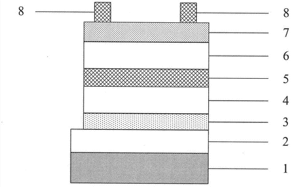
Flexible-substrate iron silicide (beta-FeSi2) thin-film solar battery and preparation method thereof
A thin-film solar cell and flexible substrate technology, which is applied in the field of solar cells, can solve the problems of high material cost and unfavorable market application of battery products, and achieve high conversion efficiency, prevent interdiffusion of elements, and simple preparation methods
- Summary
- Abstract
- Description
- Claims
- Application Information
AI Technical Summary
Problems solved by technology
Method used
Image
Examples
Embodiment 1
[0030] Refer to attached figure 1 , to prepare flexible β-FeSi 2 The manufacture method of thin-film solar cell comprises the steps:
[0031] Step 1. On the stainless steel foil substrate, deposit a Mo film on the back electrode by DC pulse magnetron sputtering with a thickness of 500nm to 900nm. The atmosphere during sputtering is Ar gas, and the vacuum degree of the atmosphere is 0.5Pa to 1Pa;
[0032] Step 2, using radio frequency magnetron sputtering Si target, depositing a Si thin layer with a thickness of 3nm-10nm on the back electrode, and the purity of the Si target material is above 99.99%. In the subsequent rapid thermal annealing process in a vacuum environment, MoSi is formed on the back electrode through the interdiffusion reaction of Mo and Si. 2 Membrane transition layer, MoSi 2 The film thickness is 10 nm to 20 nm. The rapid thermal annealing temperature is 500° C. to 750° C., and the annealing treatment time is 3 seconds to 10 seconds.
[0033] Step 3. Us...
Embodiment 2
[0038] In the above step 3 and step 5, the Fe—Si film can be deposited by intermediate frequency magnetron sputtering. All the other steps are the same as in Example 1.
Embodiment 3
[0040] In the above step 1, two layers of Mo films may be deposited on the stainless steel foil substrate by using DC pulse magnetron sputtering, with a total thickness of 500nm-900nm. On the stainless steel foil substrate, a Mo film with a thickness of 30nm-100nm is deposited by sputtering, the atmosphere is Ar gas during sputtering, and the vacuum degree of the atmosphere is 0.8Pa-0.9Pa. Then, a Mo film with a thickness of 700nm-800nm is deposited by sputtering, the atmosphere is Ar gas during sputtering, and the vacuum degree of the atmosphere is 0.5Pa-0.6Pa. The bilayer Mo film has a (110) preferred orientation, which is conducive to the subsequent preparation of high-quality β-FeSi 2 film. All the other steps are the same as in Example 1.
PUM
| Property | Measurement | Unit |
|---|---|---|
| thickness | aaaaa | aaaaa |
| thickness | aaaaa | aaaaa |
| thickness | aaaaa | aaaaa |
Abstract
Description
Claims
Application Information
