Method for preparing black silicon by metallic copper ion auxiliary etching

An ion-assisted, metallic copper technology, used in semiconductor/solid-state device manufacturing, electrical components, circuits, etc., can solve the problem of nanowire structure unfavorable photo-generated carrier collection, difficult to prepare good contact metal electrodes, and reduce photovoltaic device conversion efficiency, etc. problems, to achieve the effect of large-area production, easy cleaning, and improved conversion efficiency

Inactive Publication Date: 2012-11-07
NANJING UNIV
View PDF2 Cites 23 Cited by
  • Summary
  • Abstract
  • Description
  • Claims
  • Application Information

AI Technical Summary

Problems solved by technology

[0006] However, the current mainstream process for preparing black silicon by metal-assisted etching requires the use of precious metals such as platinum, gold, and silver. Not only is the cost high, but the precious metals are not easy to clean. Impurities are introduced into photovoltaic devices, reducing the conversion efficiency of photovoltaic d

Method used


Image

  • Method for preparing black silicon by metallic copper ion auxiliary etching
  • Method for preparing black silicon by metallic copper ion auxiliary etching
  • Method for preparing black silicon by metallic copper ion auxiliary etching

Examples


Embodiment 1

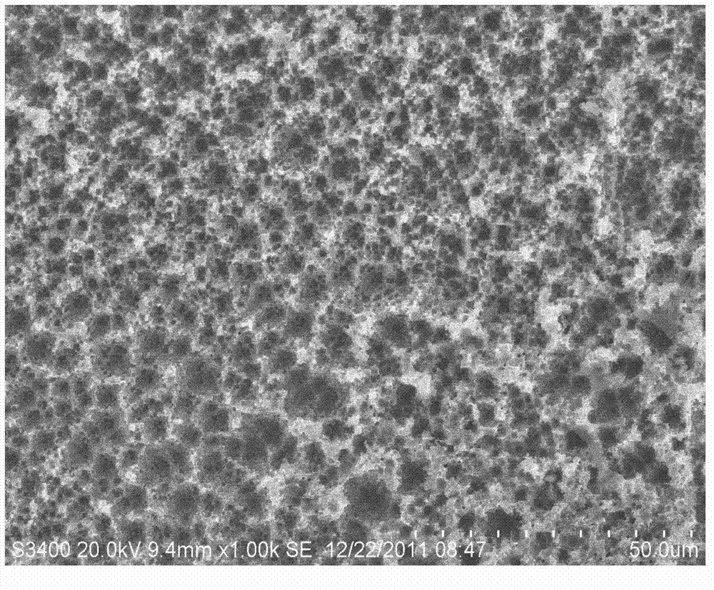
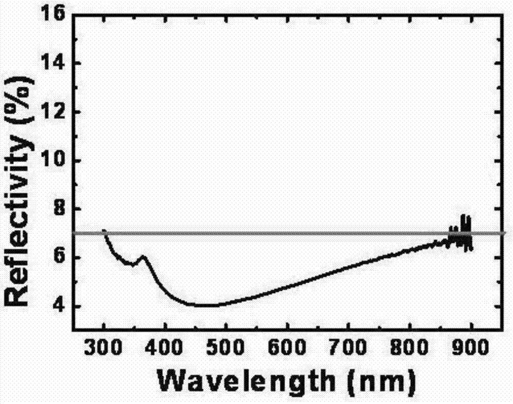
[0025] Embodiment 1: configure 100 milliliters mixed solution by the mol ratio 5:4 of hydrofluoric acid and hydrogen peroxide, wherein the concentration of hydrofluoric acid is 5 mol / L, and the concentration of hydrogen peroxide is 4 mol / L, and the concentration of copper nitrate The concentration is 0.02 mol / L. Put the unpolished polycrystalline silicon chip into the solution at room temperature or 25 ℃, take out the silicon chip after 15 minutes, wash it with concentrated nitric acid solution, rinse it with deionized water and dry it. The prepared black silicon material absorbs more than 93% of the light in the wavelength range of 300-900nm. The SEM top view of black silicon material is as follows figure 1 As shown, a relatively uniform circular microporous structure is formed on the surface of the black silicon material. figure 2 It shows that the light absorption of the black silicon material in the wavelength range of 300-900nm is as high as 93%. If the ratio of the ...

Embodiment 2

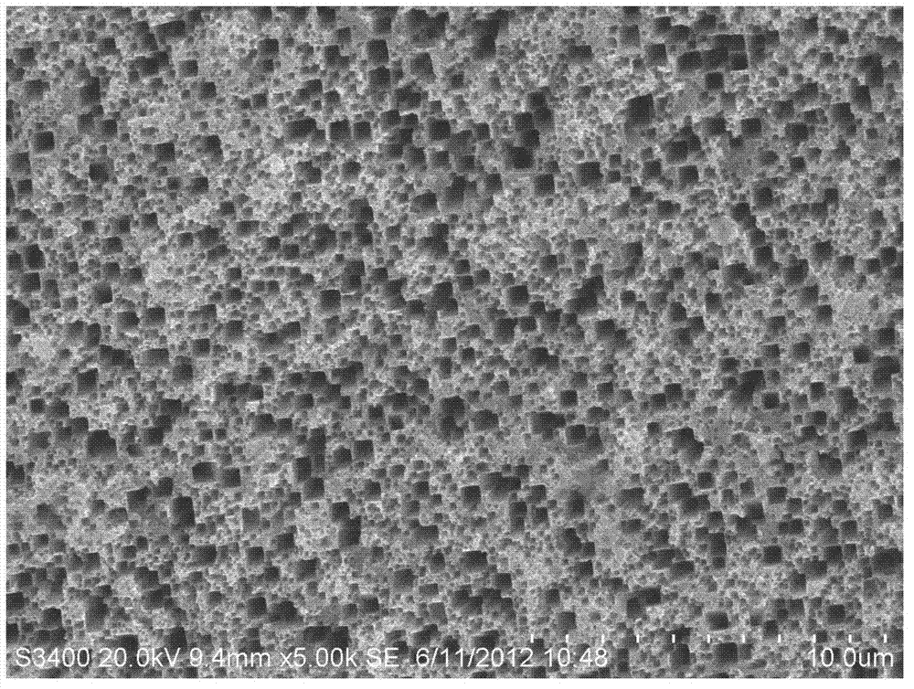
[0026] Embodiment 2: configure 100 milliliters mixed solution by the mol ratio 2:4 of hydrofluoric acid and hydrogen peroxide, wherein the concentration of hydrofluoric acid is 2 mol / L, and the concentration of hydrogen peroxide is 4 mol / L, and the concentration of copper nitrate The concentration is 0.04 mol / L. Put the unpolished polycrystalline silicon chip into the solution heated to 40 ℃, take out the silicon chip after 60 minutes, wash it with concentrated nitric acid solution, rinse it with deionized water and dry it. The prepared black silicon material absorbs more than 92% of the light in the wavelength range of 400-900nm. The SEM top view of black silicon material is as follows image 3 As shown, a relatively uniform square nanopore structure is formed on the surface of the black silicon material. Figure 4 It shows that the light absorption of the black silicon material in the wavelength range of 400-900nm is as high as 92%. The concentration of hydrofluoric acid ...

Embodiment 3

[0027] Embodiment 3: configure 100 milliliters mixed solutions by the mol ratio 5:4 of hydrofluoric acid and hydrogen peroxide, wherein the concentration of hydrofluoric acid is 5 mol / L, and the concentration of hydrogen peroxide is 4 mol / L, and the concentration of copper nitrate The concentration is 0.2 mol / L. Put the unpolished polysilicon chip into the solution cooled to 5 ℃, take out the silicon chip after 120 minutes, wash it with concentrated nitric acid or concentrated sulfuric acid solution, rinse it with deionized water and dry it. The SEM top view of black silicon material is as follows figure 1 As shown, the surface of the black silicon material forms a relatively uniform micro-hole structure.


PUM


Abstract

The invention discloses a method for preparing black silicon by using metallic copper ion auxiliary etching, comprising the following steps of (1) preparing an etchant solution which is a mixed solution composed of hydrofluoric acid, hydrogen peroxide and cupric nitrate; (2) placing a monocrystalline or polycrystalline silicon wafer into the etchant solution which contains metallic copper ions, and controlling the temperature of the etchant solution and the reaction time; and (3) taking out the reacted silicon wafer, washing the silicon wafer with an oxidative acid liquor to remove metallic residues, washing, with ionized water, and drying the silicon wafer so as to obtain a black silicon material. Monocrystalline or polycrystalline silicon surfaces are etched in a texturing manner by the catalytic action of the metal copper ions, and the black silicon material with uniform nano-pores at the surface is prepared, so that the reflectivity of monocrystalline or polycrystalline silicon materials in a light absorption waveband is obviously reduced, and conversion efficiency of silicon-based solar cells is improved.

Description

technical field [0001] The invention discloses a method for preparing black silicon by metal ion assisted etching, in particular to a method for texturing the surface of single crystal silicon or polycrystalline silicon by metal copper ion assisted etching, and belongs to the technical field of semiconductor optoelectronic material preparation. Background technique [0002] Since the advent of practical photovoltaic cells in 1954, crystalline silicon photovoltaic cells have accounted for more than 90% of the total output of photovoltaic cells due to their extremely rich raw material reserves, stable device performance, and long service life. How to further reduce the power generation cost of silicon-based photovoltaic cells and make it a renewable energy source with cost-competitive advantages is of great significance. [0003] Texturing the surface of crystalline silicon to form black silicon can greatly reduce the reflection loss of light in the absorption band on the sili...

Claims


Application Information

Patent Timeline
IPC IPC(8): H01L21/306
Inventor 王申虞栋邹文琴张凤鸣吴小山
Owner NANJING UNIV
Why Eureka
Try Eureka