Gallium nitride-based hetero-junction field effect transistor with back electrode structure

A heterojunction field effect, gallium nitride-based technology, applied in circuits, electrical components, semiconductor devices, etc., can solve problems such as the inability to reach the withstand voltage limit of GaN materials, and improve device breakdown voltage, suppress leakage current, The effect of uniform electric field distribution

Active Publication Date: 2012-12-12
UNIV OF ELECTRONICS SCI & TECH OF CHINA
View PDF5 Cites 25 Cited by
  • Summary
  • Abstract
  • Description
  • Claims
  • Application Information

AI Technical Summary

Problems solved by technology

but for figure 2 For the common RESURF GaN HFET shown, when the device is in reverse bias, the reverse bias voltage between the two-dimensional electron gas channel and the P-type buffer layer is not enough to make the channel two-dimensional electron gas and the P-type buffer layer Completely depleted, so that the withstand voltage limit of GaN material cannot be reached

Method used


Image

  • Gallium nitride-based hetero-junction field effect transistor with back electrode structure
  • Gallium nitride-based hetero-junction field effect transistor with back electrode structure
  • Gallium nitride-based hetero-junction field effect transistor with back electrode structure

Examples


Embodiment

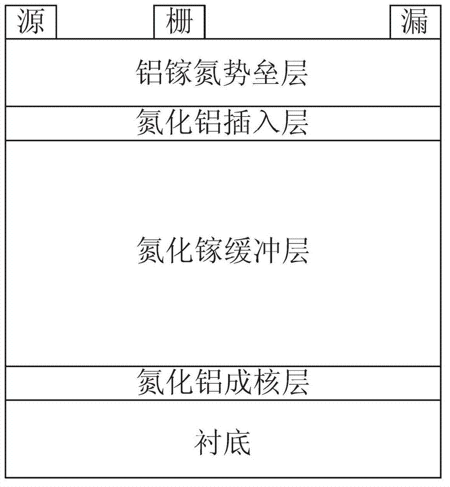
[0030] figure 1 It is a schematic diagram of the existing GaN HFET structure, mainly including a substrate, an aluminum nitride (AlN) nucleation layer, a gallium nitride (GaN) buffer layer, an aluminum nitride (AlN) insertion layer, and an aluminum gallium nitride (AlGaN) barrier layer and the source, drain and gate formed on the aluminum gallium nitride (AlGaN) barrier layer, wherein the source and drain form ohmic contacts with the aluminum gallium nitride (AlGaN) barrier layer, and the gate is in contact with the aluminum gallium nitride (AlGaN) barrier layer AlGaN) barrier layer forms a Schottky contact.

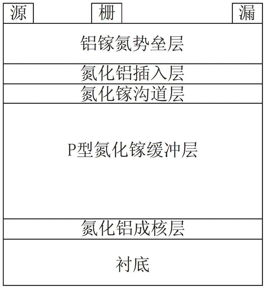
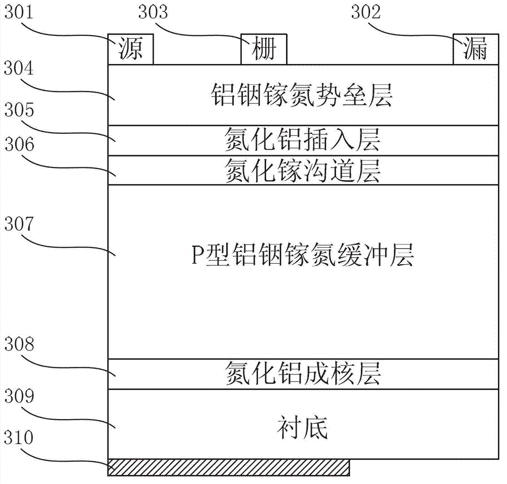
[0031] figure 2 It is an existing technology RESURF GaN HFET structure, mainly including substrate, aluminum nitride (AlN) nucleation layer, P-type gallium nitride (GaN) buffer layer, gallium nitride (GaN) channel layer, aluminum nitride (AlN) ) insertion layer, aluminum gallium nitride (AlGaN) barrier layer and the source, drain and gate formed on the aluminum galliu...


PUM


Abstract

The invention discloses a gallium nitride-based hetero-junction field effect transistor with a back electrode structure. The gallium nitride-based hetero-junction field effect transistor mainly consists of a substrate, an aluminum nitride nucleating layer, a P-type aluminum-indium-gallium-nitrogen buffering layer, a gallium nitride channel layer, an aluminum nitride inserting layer and an aluminum-indium-gallium-nitrogen barrier layer in sequence from bottom to top; a source electrode, a drain electrode and a gate electrode are formed on the barrier layer; the source electrode and the drain electrode form ohmic contact with the barrier layer; the gate electrode and the barrier layer are in Schottky contact; and the gallium nitride-based hetero-junction field effect transistor further comprises the back electrode in contact with the substrate. The back electrode in the gallium nitride-based hetero-junction field effect transistor provided by the invention modulates potential distribution of a device buffering layer, so as to increase potential difference between the two-dimensional electron gas channel and the P-type aluminum-indium-gallium-nitrogen buffering layer. Therefore, two-dimensional electron gas in the channel and the P-type impurities in the buffering layer are entirely consumed, so that the electric field distribution of the device channel is more uniform, and the breakdown voltage of the device is improved.

Description

technical field [0001] The invention relates to the field of semiconductor devices, in particular to a gallium nitride (GaN)-based heterojunction field effect transistor with a back electrode structure. Background technique [0002] Gallium nitride (GaN) based heterojunction field effect transistor has excellent characteristics such as large band gap, high critical breakdown electric field, high electron saturation velocity, good thermal conductivity, radiation resistance and good chemical stability. (GaN) materials can form two-dimensional electron gas heterojunction channels with high concentration and high mobility with materials such as aluminum gallium nitride (AlGaN), so they are especially suitable for high-voltage, high-power and high-temperature applications, and are the most suitable for power electronics applications. One of the most promising transistors. [0003] figure 1 It is a schematic diagram of a common GaN HFET structure in the prior art, mainly includi...

Claims


Application Information

Patent Timeline
Patent Type & Authority Applications(China)
IPC IPC(8): H01L29/40H01L29/778
Inventor 杜江峰赵子奇尹江龙张新川马坤华罗谦于奇
Owner UNIV OF ELECTRONICS SCI & TECH OF CHINA
Why Eureka
Try Eureka