Supercharge Your Innovation With Domain-Expert AI Agents!

Oxide for semiconductor layer of thin-film transistor, sputtering target, and thin-film transistor

A thin-film transistor and oxide technology, applied in the manufacture of transistors, semiconductor devices, semiconductor/solid-state devices, etc., can solve the problems of reduced conductivity, change in switching characteristics, and reduced reliability, and achieve excellent switching characteristics, excellent stress tolerance, Reliable effect

Active Publication Date: 2015-06-24
SAMSUNG DISPLAY CO LTD
View PDF7 Cites 0 Cited by
  • Summary
  • Abstract
  • Description
  • Claims
  • Application Information

AI Technical Summary

Problems solved by technology

For example, when a positive or negative voltage is continuously applied to the gate voltage, and when the blue wavelength band where light absorption starts is continuously irradiated, the threshold voltage changes greatly (drift), but this indicates that the switching characteristics of the TFT change.
In addition, when the liquid crystal panel is driven or when the pixel is turned on by applying a negative bias to the gate electrode, the light leaked from the liquid crystal cell is irradiated to the TFT, but this light exerts stress on the TFT and causes deterioration of characteristics.
In particular, threshold voltage shifts lead to a decrease in the reliability of display devices such as TFT-equipped liquid crystal displays and organic EL displays. Therefore, improvement in stress resistance (less change before and after stress application) is desired.
[0009] However, in ZTO-based oxide semiconductors, there is a problem that the carrier concentration tends to be high, and when the protective film (insulating film) of the TFT element is formed, the semiconductor layer becomes conductive, and stable switching performance cannot be obtained.
In order to obtain stable switching performance, although there is a method of reducing the concentration of ZnO in the ZTO-based oxide semiconductor, if the concentration of ZnO is too low, the conductivity of the sputtering target of the ZTO-based oxide semiconductor will decrease, and it will be difficult to adopt a simple structure of the device. and easy-to-control DC sputtering method for film formation

Method used


Image

  • Oxide for semiconductor layer of thin-film transistor, sputtering target, and thin-film transistor
  • Oxide for semiconductor layer of thin-film transistor, sputtering target, and thin-film transistor
  • Oxide for semiconductor layer of thin-film transistor, sputtering target, and thin-film transistor

Examples


Embodiment 1

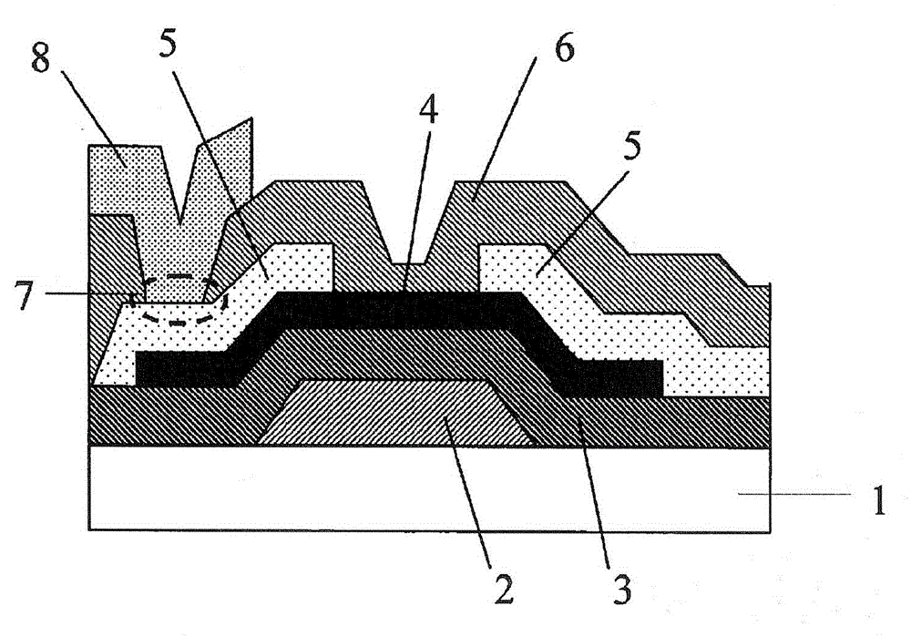
[0075] Based on the aforementioned method, the production figure 1 For the thin film transistor (TFT) shown, the TFT characteristics before and after the formation of the protective film were evaluated.

[0076] First, on a glass substrate (Igre 2000 manufactured by Corning Corporation, 100 mm in diameter x 0.7 mm in thickness), as a gate electrode, a Ti thin film of 100 nm and a gate insulating film of SiO were sequentially deposited. 2 (200nm). A pure Ti sputtering target was used for the gate electrode, and a film was formed by a DC sputtering method at a film forming temperature: room temperature, a film forming power: 300W, a carrier gas: Ar, and a gas pressure: 2mTorr. In addition, the gate insulating film uses the plasma CVD method with a carrier gas: SiH 4 and N 2 A mixed gas of O, a film forming power: 100 W, and a film forming temperature: 300° C. were used to form a film.

[0077] Next, oxide thin films having various compositions described in Table 1 were forme...

Embodiment 2

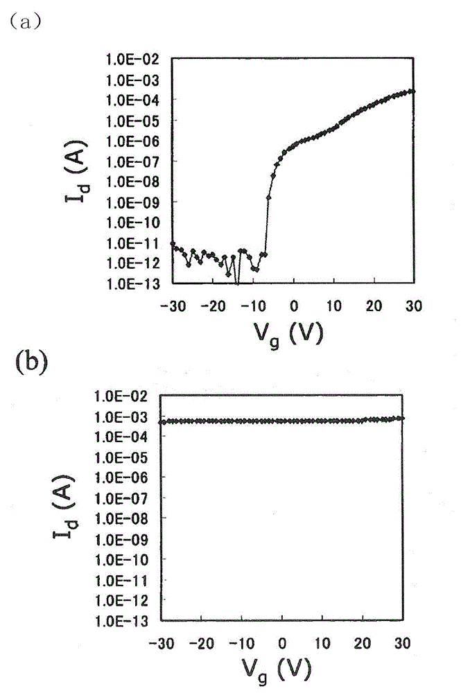
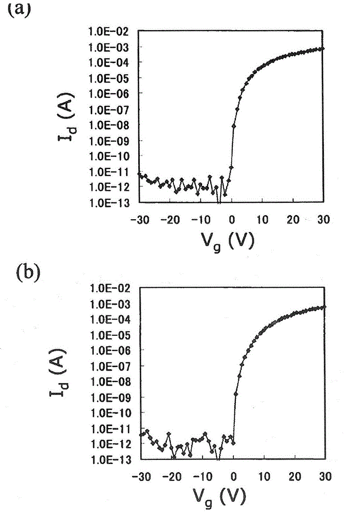
[0126] In this example, each TFT produced in the same manner as in Example 1 using various oxide thin films described in Table 1 and Table 2 was evaluated in the following manner (4) Stress tolerance before and after stress application.

[0127] (4) Evaluation of stress tolerance (light irradiation + negative bias applied as stress)

[0128] In the present example, a stress application test in which light is irradiated while applying a negative bias to the gate electrode is performed by simulating the environment (stress) at the time of actual panel driving. Stress application conditions are as follows. As the wavelength of light, select about 400 nm, which is close to the bandgap of the oxide semiconductor, and the transistor characteristics are likely to fluctuate.

[0129] Gate voltage: -20V

[0130] Drain voltage: 10V

[0131] Substrate temperature: 60°C

[0132] light stress

[0133] Wavelength: 400nm

[0134] Illuminance (intensity of light irradiated to TFT): 80nW...

Embodiment 3

[0160] In this embodiment, the oxide corresponding to No.3 composition of Table 3 (ZnSnO+3at%Al, [Zn]:[Sn]=6:4, Zn ratio=[Zn] / [Zn]+[ Sn]=0.6, Al ratio=[Al] / [Zn]+[Sn]+[Al]=0.03), the oxide film ( The film thickness was 100 nm), and the mobility and the threshold voltage change (ΔVth) after the stress test (external light irradiation + negative bias) were investigated for the TFT fabricated in the same manner as in Example 2 above. The method of measuring the film density is as follows.


PUM


Abstract

Disclosed is an oxide for a semiconductor layer of a thin-film transistor, said oxide being excellent in the switching characteristics of a thin-film transistor, specifically enabling favorable characteristics to be stably obtained even in a region of which the ZnO concentration is high and even after forming a passivation layer and after applying stress. The oxide is used in a semiconductor layer of a thin-film transistor, and the aforementioned oxide contains Zn and Sn, and further contains at least one element selected from group X consisting of Al, Hf, Ta, Ti, Nb, Mg, Ga, and the rare-earth elements.

Description

technical field [0001] The present invention relates to an oxide for a semiconductor layer of a thin film transistor used in display devices such as a liquid crystal display and an organic EL display, and a sputtering target and a thin film transistor for forming the oxide. Background technique [0002] Compared with general-purpose amorphous silicon (a-Si), amorphous (amorphous) oxide semiconductors have high carrier mobility, a large optical band gap, and can be formed at low temperatures, so they are expected to meet the needs of Applications such as large-scale / high-resolution / high-speed drive epoch-making displays and resin substrates with low heat resistance. [0003] Examples of oxide semiconductors include In-containing amorphous oxide semiconductors (In-Ga-Zn-O, In-Zn-O, etc.), but the use of In, which is a rare metal, requires Worried about rising material costs. Therefore, as an oxide semiconductor that does not contain In, can reduce material costs, and is suit...

Claims


Application Information

Patent Timeline
Patent Type & Authority Patents(China)
IPC IPC(8): H01L29/786H01L21/363
CPCH01L21/02422H01L21/02554H01L21/02565H01L21/02631H01L29/78693H01L29/66969H01L29/7869H01L29/26H01L29/66742
Inventor 三木绫岩成裕美钉宫敏洋森田晋也寺尾泰昭安野聪朴在佑李制勋安秉斗
Owner SAMSUNG DISPLAY CO LTD
Features
  • R&D
  • Intellectual Property
  • Life Sciences
  • Materials
  • Tech Scout
  • Unparalleled Data Quality
  • Higher Quality Content
  • 60% Fewer Hallucinations
Learn More