

Preparation method for graphene
A graphene and semiconductor technology, applied in the field of graphene and graphene preparation by chemical vapor deposition, can solve the problems of inability to prepare layers of high-quality graphene, achieve the effect of eliminating quality defects and simplifying the preparation process
- Summary
- Abstract
- Description
- Claims
- Application Information
AI Technical Summary
Problems solved by technology
Method used
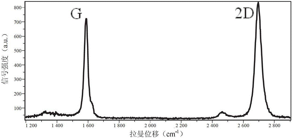
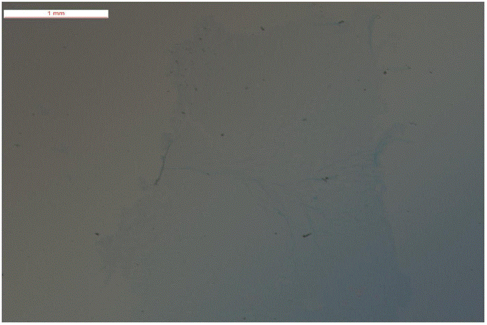
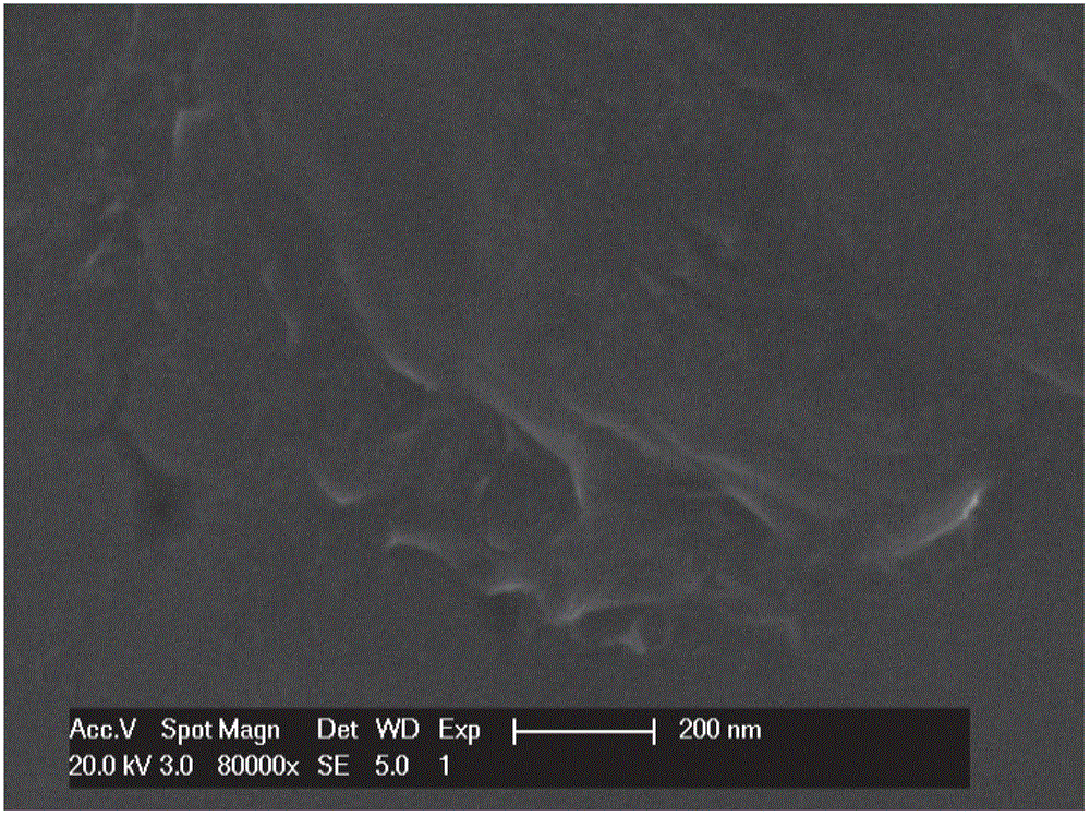
Image

Examples
Embodiment 1
[0033] The invention provides a kind of preparation method of graphene, described method comprises at least:
[0034] First perform step 1) providing a semiconductor substrate as a catalyst. Preferably, the semiconductor substrate is cleaned with water, deionized water, ethanol and acetone in sequence, wherein the semiconductor substrate includes germanium or gallium arsenide. In the first embodiment, since the semiconductor substrate is a no-clean germanium material substrate, the cleaning step is not required. Then go to step 2).
[0035] In step 2), under hydrogen and an inert atmosphere, the semiconductor substrate is heated to 810-910°C in a tube furnace, the flow rate of the hydrogen gas is 2-50 sccm, preferably, the flow rate of the hydrogen gas is 30 ~50 sccm. Specifically, in the first embodiment, hydrogen and argon (Ar) are selected as the hydrogen gas and the inert atmosphere, wherein the flow rate of hydrogen gas is 50 sccm, and the flow rate of argon gas is 200 ...
Embodiment 2
[0047] The technical scheme of the preparation method of Example 2 is basically the same as that of Example 1, the only difference is that in this Example 2, only the flow rate of the carbon source in step 3) is adjusted, which are respectively selected from 3sccm, 2sccm, 0.75sccm, 0.1sccm sccm four situations, and compare the graphene prepared under these four different reaction parameter conditions, and for the rest of the similarities, please refer to the relevant description of Example 1.
[0048] The rest of the reaction parameters in Example 2 except the carbon source flow rate are the same as in Example 1, specifically: the semiconductor substrate is germanium, the heating temperature (i.e. reaction temperature) for the germanium semiconductor substrate is 910°C, and the hydrogen flow rate is 50 sccm. The inert gas is argon (Ar) with a flow rate of 200 sccm, the reaction time is 100 min, and the carbon source is gaseous carbon source methane.
[0049] It should be noted...
Embodiment 3
[0052] The technical solution of the preparation method of the third embodiment is basically the same as that of the first embodiment, the only difference is that in the third embodiment only the heating temperature (reaction temperature) of the semiconductor substrate is adjusted, which are respectively selected from 810°C, 850°C, 900°C °C and 910 °C, and compare the graphene prepared under these four different reaction parameter conditions. For other similarities, please refer to the relevant description of Example 1.
[0053]Except for the heating temperature (reaction temperature) of the semiconductor substrate in the third embodiment, the remaining reaction parameters are the same as those in the first embodiment, specifically: the semiconductor substrate is germanium, the flow rate of hydrogen is 50 sccm, the inert gas is argon (Ar) and The flow rate is 200 sccm, the reaction time is 100 min, the carbon source is gaseous carbon source methane, and the flow rate of methane...
PUM
 Abstract
Description
Claims
Application Information