Manufacturing method of Terahertz Schottky diode

A manufacturing method and diode technology, applied in semiconductor/solid-state device manufacturing, electrical components, circuits, etc., can solve the problems of reducing the mixing efficiency of mixers and increasing frequency conversion losses, so as to reduce discontinuity and parasitic capacitance , The effect of reducing thermal electron noise

Active Publication Date: 2013-01-23
孙琦
View PDF5 Cites 21 Cited by
  • Summary
  • Abstract
  • Description
  • Claims
  • Application Information

AI Technical Summary

Problems solved by technology

However, due to the high frequency in the terahertz band, many high-frequency spurious effects w

Method used


Image

  • Manufacturing method of Terahertz Schottky diode
  • Manufacturing method of Terahertz Schottky diode
  • Manufacturing method of Terahertz Schottky diode

Examples


Embodiment Construction

[0031] In order to make the purpose, technical solutions and advantages of the present invention clearer, the technical solutions of the exemplary embodiments of the present invention are described below in conjunction with the accompanying drawings. Apparently, the described embodiments are only some of the embodiments of the present invention, not all of them. The described embodiments are for illustration only and do not limit the scope of the invention. Based on the embodiments of the present invention, all other embodiments obtained by persons of ordinary skill in the art without creative efforts fall within the protection scope of the present invention.

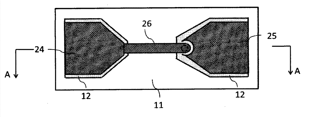
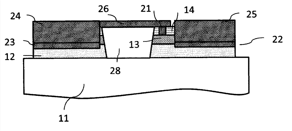
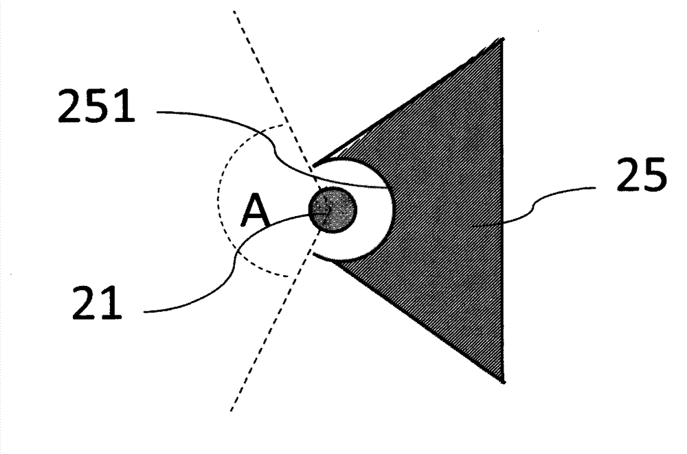
[0032] For the sake of narrative, the terms "upper", "lower" and attached figure 2 The up and down directions are the same, but it does not limit the structure of the present invention.

[0033] Although words first, second, etc. are used in this application to describe various elements or constituents, these element...


PUM


Abstract

The invention provides a manufacturing method of a Terahertz Schottky diode. The manufacturing method comprises: a high-concentration gallium arsenide-doped layer and a low-concentration gallium arsenide-doped layer are sequentially formed on a substrate of a gallium arsenide semiconductor; an Ohmic contact cathode and Ohmic contact metals are formed on the high-concentration gallium arsenide-doped layer; a silicon dioxide layer with small bores is formed on the low-concentration gallium arsenide-doped layer; a Schottky contact anode is formed; an Ohmic contact cathode pressure point, a Schottky contact anode extension pressure point and a suspending plating bridge are formed; and the Schottky contact anode extension pressure point is connected with the Schottky contact anode through the impending plating bridge. According to the Schottky diode manufactured by the manufacturing method provided by the invention, parasitic effects are reduced, thermionic noises existing in n+GaAs, the discontinuity of the anode pressure point to the impending plating bridge and the series resistance of the diode can be lowered, and the integration with peripheral circuits is easily realized by using flip chip bonding.

Description

technical field [0001] The present invention relates to semiconductor devices, and more particularly, to a terahertz Schottky diode and a manufacturing method thereof. Background technique [0002] Terahertz waves refer to electromagnetic radiation with a frequency in the range of 0.1 THz to 10 THz (wavelength 3 mm to 30 μm), which is located between millimeter waves and infrared radiation in the electromagnetic spectrum. The unique performance of terahertz makes it widely used in communication (broadband communication), radar, electronic countermeasures, electromagnetic weapons, astronomy, medical imaging (unmarked genetic inspection, imaging at the cellular level), nondestructive testing, security inspection (biochemical inspection) and other fields have a wide range of uses. In most terahertz application fields, the heterodyne receiver has become the main terahertz signal detection method due to its high spectral resolution, large instantaneous bandwidth, and high sensit...

Claims


Application Information

Patent Timeline
IPC IPC(8): H01L21/329H01L21/28
Inventor 王昊
Owner 孙琦
Why Eureka
Try Eureka