P-type amorphous silicon carbon-nanoparticle silicon multi-quantum well window layer material

An amorphous silicon carbon and nanoparticle technology, applied in photovoltaic power generation, electrical components, circuits, etc., can solve the problems of decreased structural order, wide band gap, difficult high conductivity performance, decreased conductivity, etc. Response and short-circuit current density, reduced light absorption loss, enhanced effect of built-in electric field

Inactive Publication Date: 2013-01-30
NANKAI UNIV
View PDF4 Cites 6 Cited by
  • Summary
  • Abstract
  • Description
  • Claims
  • Application Information

AI Technical Summary

Problems solved by technology

However, as the carbon content and band gap in the amorphous silicon carbon film increase, the doping efficiency will decrease and the electrical conductivity will decrease; on the other hand, the electrical conductivity of the p-type amorphous silicon carbon material can be improved by increasing the gas phase doping concentration. At this time, the structural order of the material is severely reduced, resulting in a decrease in the band gap.
In short, the band gap, carbon content, conductivity, doping concentration and other factors of traditional p-type amorphous silicon carbon materials restrict each other, making it difficult to obtain wide band gap and high conductivity properties at the same time, which ultimately affects the improvement of the overall performance of solar cells.

Method used


Image

  • P-type amorphous silicon carbon-nanoparticle silicon multi-quantum well window layer material
  • P-type amorphous silicon carbon-nanoparticle silicon multi-quantum well window layer material
  • P-type amorphous silicon carbon-nanoparticle silicon multi-quantum well window layer material

Examples


Embodiment

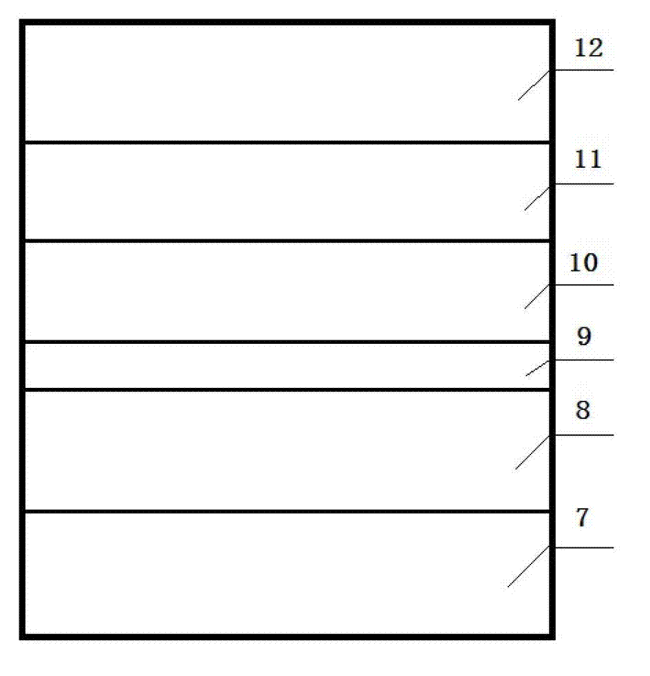
[0023] A p-type amorphous silicon carbon-nanoparticle silicon multiple quantum well window layer material, such as figure 1 As shown, it is a multi-layer material prepared by the layer-by-layer deposition method, which is alternately grown by wide-bandgap amorphous silicon-carbon films and narrow-bandgap p-type nanoparticle silicon films. Amorphous silicon-carbon films 1, 3, and 5 are plasma-enhanced The chemical vapor deposition technology is prepared under the condition that the substrate temperature is 150°C. The reaction gas is a mixed gas of silane, methane and hydrogen, and the volume flow percentage is: silane accounts for 0.5%, methane accounts for 4.5%, hydrogen is the balance, and amorphous silicon The thickness of the carbon film is 5nm, and the carbon content in the film is 70%. The p-type nanoparticle silicon films 2, 4, and 6 are prepared by plasma-enhanced chemical vapor deposition at a substrate temperature of 75°C, and the glow power density is 0.75W / cm 2 , t...


PUM

PropertyMeasurementUnit
thicknessaaaaaaaaaa
band gapaaaaaaaaaa
electrical conductivityaaaaaaaaaa

Abstract

The invention discloses a p-type amorphous silicon carbon-nanoparticle silicon multi-quantum well window layer material. The p-type amorphous silicon carbon-nanoparticle silicon multi-quantum well window layer material is a multilayer material which is prepared by using a cascading deposition method and formed by alternately growing broadband gap amorphous silicon carbon thin films and narrowband gap p-type nanoparticle silicon thin films, wherein the thickness of each amorphous silicon carbon thin film is between 2 nm and 8 nm; the thickness of each p-type nanoparticle silicon thin film is between 2 nm and 8 nm; by repeated deposition, a p-type amorphous silicon carbon-nanoparticle silicon multi-quantum well material of which the total thickness is between 20 nm and 50 nm is formed; and the p-type amorphous silicon carbon-nanoparticle silicon multi-quantum well window layer material is applicable to a silicon-based thin film solar cell. The p-type amorphous silicon carbon-nanoparticle silicon multi-quantum well window layer material has the advantages that an optical band gap can reach 2.0 to 3.7 eV, and electric conductivity can reach 0.1 to 5.0 S/cm; and the material is applicable to the silicon-based thin film solar cell, so the open-circuit voltage of the cell can be remarkably improved, the optical absorption loss of a window layer is reduced, the short wave response and short-circuit current density of the cell are improved, and photoelectric conversion efficiency is improved.

Description

【Technical field】 [0001] The invention belongs to the field of silicon-based thin-film solar cells, in particular to a p-type amorphous silicon carbon-nano particle silicon multi-quantum well window layer material. 【technical background】 [0002] Silicon-based thin-film solar cells are the most researched and most mature technology because of the abundant, non-toxic and non-polluting semiconductor material silicon used. Among them, silicon-based thin-film solar cells have become an important direction for the development of solar cells in the future due to their short industrial chain, low manufacturing cost, low energy consumption, and pollution-free manufacturing process. [0003] The p-type doped layer acts as a window layer of the silicon-based thin film battery, and together with the n-type doped layer forms a built-in electric field of the silicon-based thin film battery. The requirements for the p-type window layer are high conductivity, low activation energy and wid...

Claims


Application Information

Patent Timeline
Patent Type & Authority Applications(China)
IPC IPC(8): H01L31/0376H01L31/0352
CPCY02E10/50
Inventor 倪牮马峻张建军侯国付陈新亮张晓丹赵颖
Owner NANKAI UNIV
Why Eureka
Try Eureka