Silicon-based near infrared photoelectric detector structure and manufacturing method thereof

A technology of near-infrared light and electrical detectors, applied in circuits, electrical components, semiconductor devices, etc., can solve the problems of weak near-infrared light response, reduce leakage and background noise signals, have low surface roughness, and be easy to operate Effect

Inactive Publication Date: 2013-01-30
INST OF SEMICONDUCTORS - CHINESE ACAD OF SCI
View PDF4 Cites 22 Cited by
  • Summary
  • Abstract
  • Description
  • Claims
  • Application Information

AI Technical Summary

Problems solved by technology

[0005] The main purpose of the present invention is to propose a silicon-based near-infrared photodetector structure and its manufacturing method, to solve the problem of weak response of tradition...

Method used


Image

  • Silicon-based near infrared photoelectric detector structure and manufacturing method thereof
  • Silicon-based near infrared photoelectric detector structure and manufacturing method thereof
  • Silicon-based near infrared photoelectric detector structure and manufacturing method thereof

Examples


Embodiment Construction

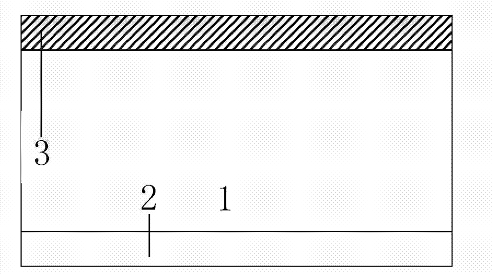
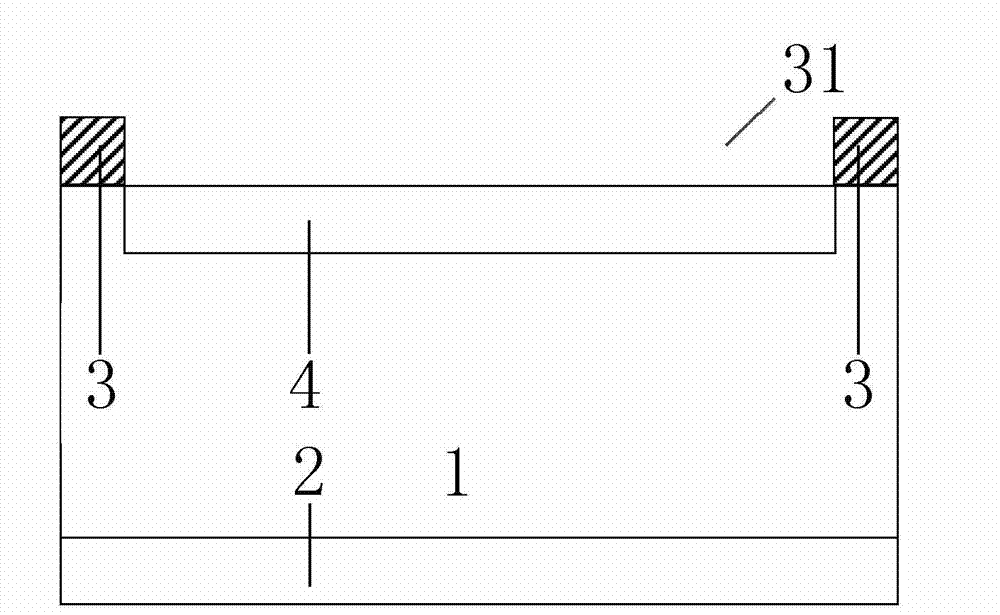
[0035] The silicon-based near-infrared photodetector structure provided by the present invention forms a pn junction at the interface between the p-type boron doped layer 4 and the n-type silicon substrate 1, and the pn junction region is activated by pulsed laser irradiation of chalcogenides The doping layer 5 enhances the absorption of near-infrared light by the silicon material, and the photogenerated electron-hole pairs are easily separated under the built-in electric field and reverse bias voltage and collected by the respective electrodes, and converted into photocurrent, which solves the traditional The problem of weak photoresponse of silicon photodetectors outside the wavelength of 1100nm has realized the near-infrared photodetection of silicon-based photodiodes.

[0036] see Figure 6 As shown, the present invention provides a silicon-based near-infrared photodetector structure, comprising:

[0037] An n-type silicon substrate 1, the upper surface of the n-type sili...


PUM

PropertyMeasurementUnit
Depthaaaaaaaaaa
Thicknessaaaaaaaaaa

Abstract

The invention discloses a silicon-based near infrared photoelectric detector structure which comprises an n type silicon substrate, a phosphorus back field, a sulfur element doping layer, a p type boron doping layer, a see-through surface masking layer, an antireflection film layer, a front contact electrode and a back contact electrode, wherein two layers of step-shaped circular grooves are downwardly arranged above the n type silicon substrate; the phosphorus back field is arranged below the n type silicon substrate; the sulfur element doping layer is arranged in the lower circular groove above the n type silicon substrate; the p type boron doping layer is arranged in the upper circular groove above the n type silicon substrate; the see-through surface masking layer is arranged around the upper circular groove above the n type silicon substrate and covers the periphery of the p type boron doping layer; a circular hole is formed in the middle of the see-through surface masking layer; a ring-shaped groove is arranged at the periphery of the circular hole and the outer diameter of the ring-shaped groove is smaller than the diameter of the upper circular groove above the n type silicon substrate; the antireflection film layer is arranged in the circular hole in the middle of the see-through surface masking layer; the front contact electrode is arranged in the ring-shaped groove on the see-through surface masking layer; and the back contact electrode is arranged below the phosphorus back field. According to the silicon-based near infrared photoelectric detector structure, the difficulty that the traditional silicon photoelectric detectors have weak response to the near infrared lights with wavelengths greater than 1100nm can be solved, and particularly, the high-sensitivity near infrared photoelectric detection for the silicon-based photoelectric detectors can be realized.

Description

technical field [0001] The invention relates to a silicon photodetector structure and a manufacturing method thereof, in particular to a silicon-based near-infrared photodetector structure and a manufacturing method thereof. Background technique [0002] Based on the well-established silicon process, crystalline silicon is widely used to fabricate microelectronic and optoelectronic devices. However, the band gap of silicon is 1.12eV, which limits the application of silicon in the near-infrared band. The peak response wavelength of the traditional silicon photodetector is around 900nm, and its sensitivity to infrared light other than the wavelength of 1100nm is very low, so it cannot be used for photoelectric detection of the communication wavelength of 1330nm and 1550nm. Germanium and III-V materials are usually used to prepare photodetectors in the near-infrared communication band, but their high cost and poor silicon process compatibility limit their application range. ...

Claims


Application Information

Patent Timeline
IPC IPC(8): H01L31/101H01L31/0288H01L31/18
CPCY02P70/50
Inventor 胡少旭韩培德李辛毅毛雪高利朋
Owner INST OF SEMICONDUCTORS - CHINESE ACAD OF SCI
Why Eureka
Try Eureka