Method for preparing silicon nanotube by taking porous silicon as substrate
A technology of silicon nanotubes and porous silicon, which is applied in the field of preparation of new materials, can solve the problems of complex preparation process and harsh reaction conditions, and achieve the effect of simple preparation process
- Summary
- Abstract
- Description
- Claims
- Application Information
AI Technical Summary
Problems solved by technology
Method used
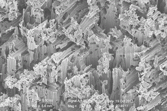
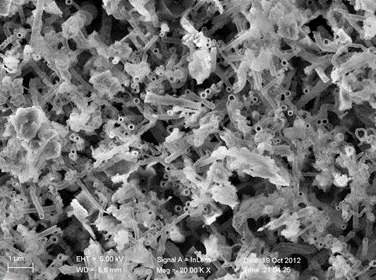
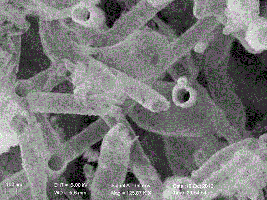
Image

Examples
Embodiment 1
[0029] (1) Take a piece of p-type double-sided polished silicon wafer, after cleaning, put it into a mixed aqueous solution of hydrofluoric acid and silver nitrate to undergo a chemical reaction, in the mixed aqueous solution: the concentration of hydrofluoric acid is 4.915M, and the concentration of silver nitrate is 0.028M, control the above etching reaction temperature to 20oC, and the reaction time to 200min;
[0030] (2) Take out the silicon chip after the above reaction, soak it in 30% nitric acid aqueous solution for 20 minutes, wash it with a large amount of deionized water, and dry it with nitrogen gas to obtain porous silicon;
[0031](3) Immerse the obtained porous silicon in a mixed aqueous solution containing hydrofluoric acid and copper ions, wherein: the concentration of hydrofluoric acid is 2M, and the concentration of copper ions is 0.001M; the reaction temperature of porous silicon in this mixed aqueous solution is 30oC , the reaction time is 200min, and the ...
Embodiment 2
[0033] (1) Take a piece of p-type double-sided polished silicon wafer, after cleaning, put it into a mixed aqueous solution of hydrofluoric acid and silver nitrate to undergo a chemical reaction, in the mixed aqueous solution: the concentration of hydrofluoric acid is 4.915M, and the concentration of silver nitrate is 0.028M, control the above etching reaction temperature to 70oC, and the reaction time to 50min;
[0034] (2) Same as step (2) of embodiment 1;
[0035] (3) Immerse the obtained porous silicon in a mixed aqueous solution of ammonium fluoride and silver ions, wherein: the concentration of sodium fluoride is 5M, and the concentration of silver ions is 0.005M; the reaction temperature of porous silicon in this mixed aqueous solution is 60oC, The reaction time is 50 min, and the product is soaked with hydrochloric acid to obtain silicon nanotubes.
Embodiment 3
[0037] (1) Take a piece of p-type double-sided polished silicon wafer, after cleaning, put it into a mixed aqueous solution of hydrofluoric acid and silver nitrate to undergo a chemical reaction, in the mixed aqueous solution: the concentration of hydrofluoric acid is 4.915M, and the concentration of silver nitrate is 0.028M, control the above etching reaction temperature to 100oC, and the reaction time to 20min;
[0038] (2) Same as step (2) of embodiment 1;
[0039] (3) Immerse the obtained porous silicon in a mixed aqueous solution of sodium fluoride and nickel ions, wherein: the concentration of ammonium fluoride is 10M, and the concentration of nickel ions is 0.01M; the reaction temperature of porous silicon in this mixed aqueous solution is 100oC, The reaction time is 30 minutes, and the product is soaked with hydrochloric acid to obtain silicon nanotubes.
[0040] The invention provides a method for preparing silicon nanotubes using porous silicon as a substrate. In t...
PUM
| Property | Measurement | Unit |
|---|---|---|
| diameter | aaaaa | aaaaa |
| length | aaaaa | aaaaa |
| diameter | aaaaa | aaaaa |
Abstract
Description
Claims
Application Information