Array substrate and manufacturing method thereof, and display device

An array substrate and manufacturing method technology, applied in the field of display, can solve the problems affecting the uniformity and stability of the common electrode network voltage, affecting the actual voltage difference of liquid crystal, and the crosstalk of the common electrode network voltage, so as to improve the display quality and coupling capacitance The effect of reducing and uniform voltage

Inactive Publication Date: 2013-03-13
BOE TECH GRP CO LTD +1
View PDF4 Cites 8 Cited by
  • Summary
  • Abstract
  • Description
  • Claims
  • Application Information

AI Technical Summary

Problems solved by technology

And because the common electrode line is generally formed at the same time as the gate metal line in the process, the two are distributed on the same layer with a certain distance between them. However, in order to maximize the transmittance of the display screen, the common electrode line is generally relatively thin, resulting in relatively low impedance. Large; at the same time, there is overlapping capacitance betw

Method used


Image

  • Array substrate and manufacturing method thereof, and display device
  • Array substrate and manufacturing method thereof, and display device
  • Array substrate and manufacturing method thereof, and display device

Examples


Example Embodiment

[0054] Example one

[0055] Combine below Figure 1 to Figure 5 , The manufacturing method of the array substrate of the present invention will be described in detail.

[0056] The manufacturing method of the array substrate in the embodiment of the present invention includes:

[0057] S1, forming a pattern including a transparent common electrode pattern and a common electrode line pattern on a base substrate;

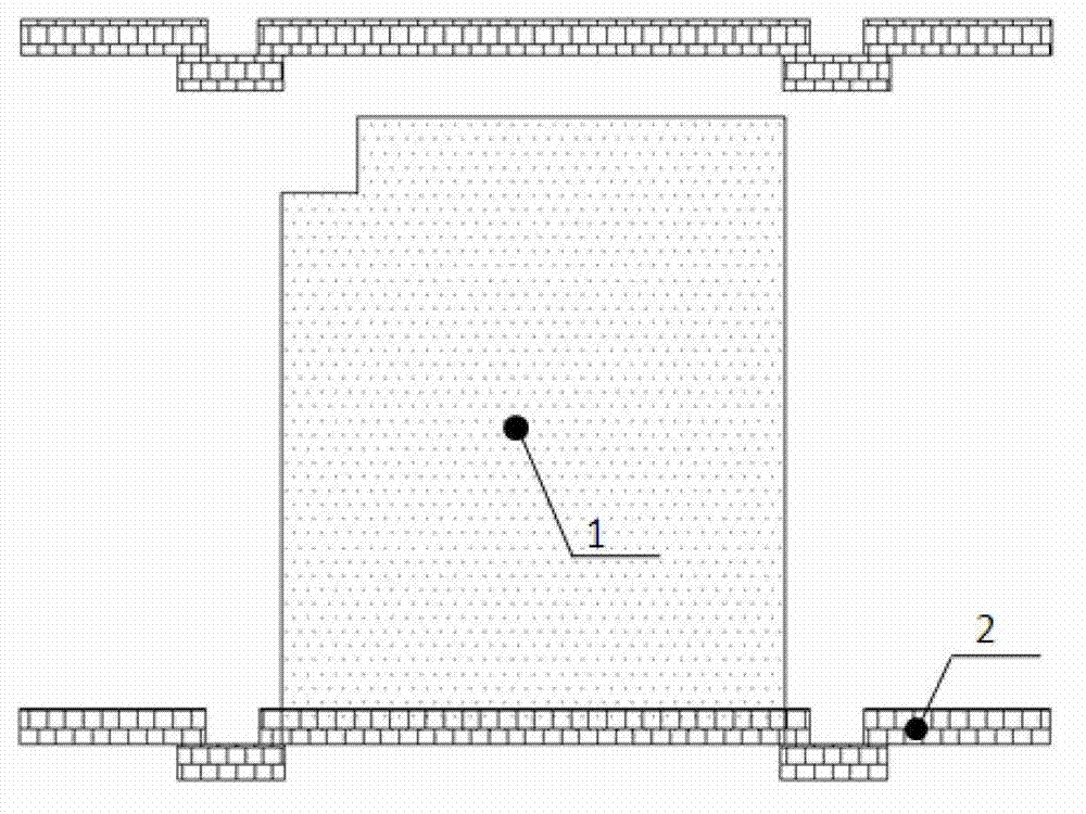
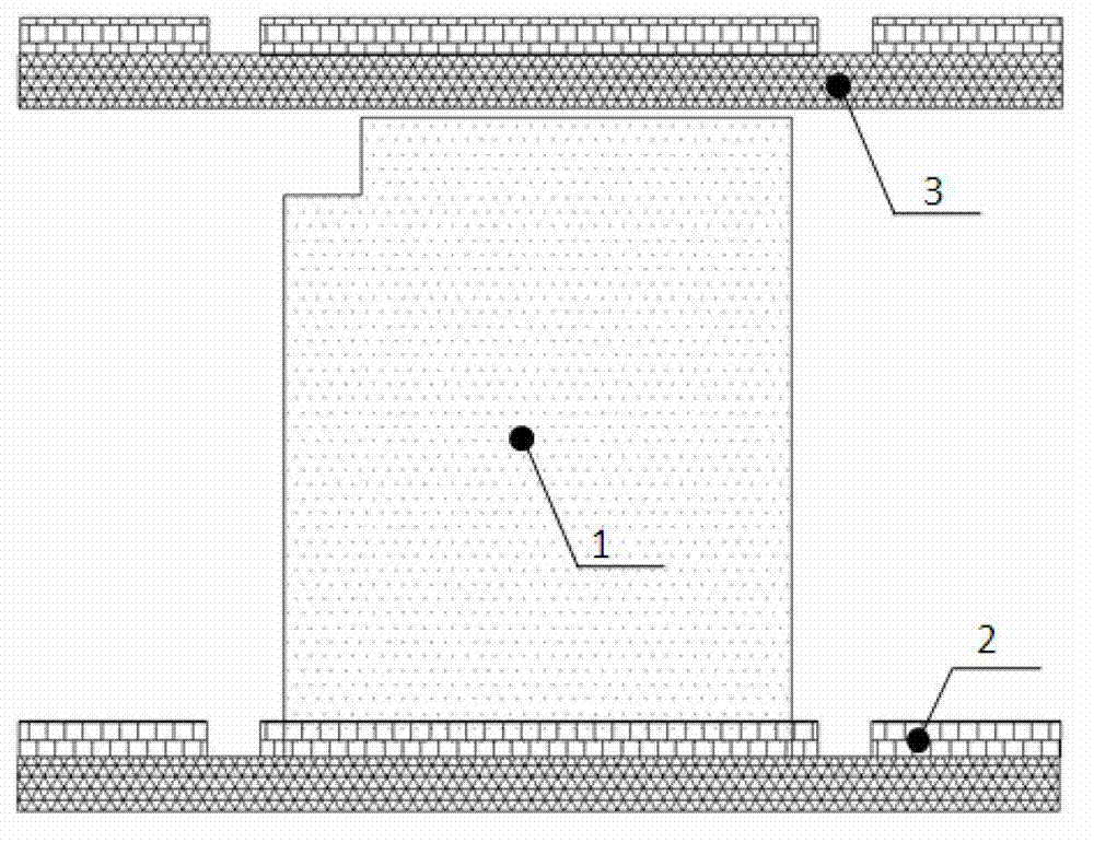
[0058] Such as Image 6 with Figure 7 As shown, the array substrate of the embodiment of the present invention is fabricated on a base substrate 8, which is usually a glass substrate, a quartz substrate or a transparent resin substrate.

[0059] A pattern including a transparent common electrode 1 and a pattern of common electrode lines 2 is formed on the base substrate 8. Specifically, first, a transparent conductive layer film (not shown in the figure) and a common electrode line metal layer film (not shown in the figure) are sequentially formed on the base substrate 8. In ...

Example Embodiment

[0100] Example two

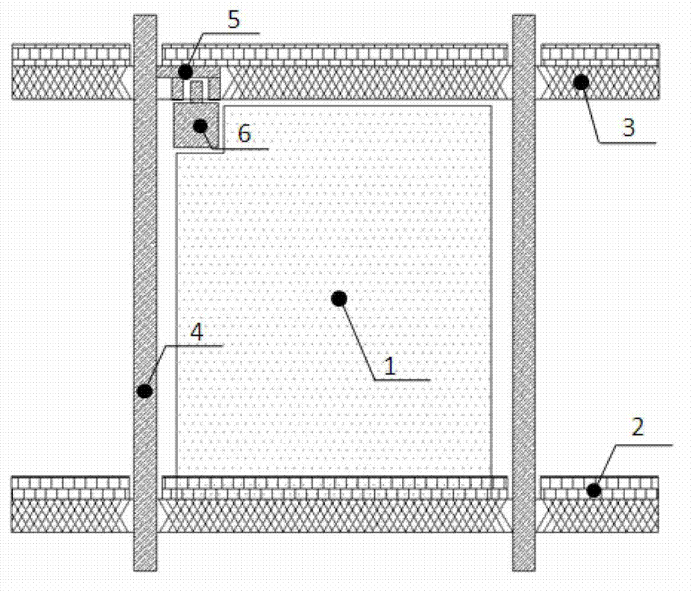
[0101] The embodiment of the present invention also provides an array substrate, including gate lines 3, data lines 4, transparent common electrodes 1 and common electrode lines 2 formed on a base substrate, and the gate lines 3 and data lines 4 are formed in the pixel area defined by the The pixel electrode 7 and the thin film transistor, wherein a common electrode insulating layer 9 is formed between the common electrode line 2 and the gate line 3, so that the common electrode line 2 and the gate line 3 are distributed in different layers, thereby improving the common electrode line 2 The line width reduces the impedance of the common electrode line, which is beneficial to the uniformity of the common electrode voltage and the rapid attenuation of voltage fluctuations.

[0102] Wherein, the overlapping area of ​​the common electrode line 2 and the data line 4 on the horizontal plane is located on both sides of the gate line 3. The above structure makes that ...

Example Embodiment

[0104] Example three

[0105] An embodiment of the present invention also provides a display device, which includes the array substrate in the second embodiment, which improves the display quality of the display device.

[0106] Among them, the display device can be any product or component with a display function, such as a liquid crystal panel, a mobile phone, a tablet computer, a TV, a monitor, a notebook computer, a digital photo frame, a navigator, and so on.


PUM


Abstract

The invention belongs to the technical field of displaying, and discloses an array substrate and a manufacturing method thereof, and a display device. According to the manufacturing method for the array substrate, the conventional thin film transistor (TFT)-liquid crystal display (LCD) array substrate manufacturing process by taking the conventional transverse electric field or multi-dimensional electric field as a drive is improved, so that public electrode wires and grid wires are distributed on different layers; therefore, on the premise that the light transmittance is not influenced, the widths of the public electrode wires are increased, the impedance of the publish electrode wires is reduced, and the uniformity and the voltage fluctuation of voltage of public electrodes can be quickly attenuated; moreover, overlap capacitance does not exist between data wires and the public electrode wires; distances between the data wires and the transparent public electrodes are enlarged; the coupling capacitance is reduced; crosstalk of a data signal on the voltage of a public electrode network is obviously reduced; the voltage of the public electrodes is uniform and stable; and the display quality is greatly improved.

Description

technical field [0001] The present invention relates to the field of display technology, in particular to an array substrate, a manufacturing method thereof, and a display device. Background technique [0002] Thin Film Transistor-Liquid Crystal Display (TFT-LCD for short) has the characteristics of small size, low power consumption, and no radiation. It has developed rapidly in recent years and occupies a dominant position in the current flat panel display market. The main structure of the TFT-LCD includes an array substrate and a color filter substrate in a box, where gate lines, data lines, and thin film transistors and pixel electrodes arranged in a matrix are formed on the array substrate. The display principle of TFT-LCD is: use the thin film transistor as a switch to apply a driving electric field to the liquid crystal to control the rotation of the liquid crystal, thereby controlling the display process of the TFT-LCD. Wherein, the driving electric field is generate...

Claims


Application Information

Patent Timeline
IPC IPC(8): H01L21/84H01L27/12G02F1/1362G02F1/1368
Inventor 刘冬陈维涛郝昭慧李承珉
Owner BOE TECH GRP CO LTD
Why Eureka
Try Eureka