Star sapphire wafer and preparation method thereof
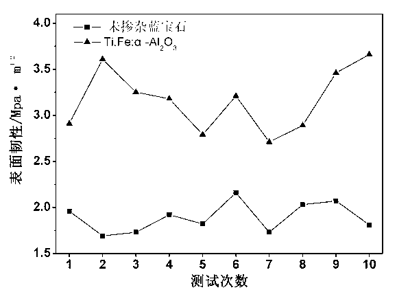
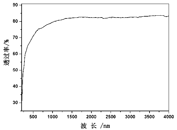
A sapphire wafer and wafer technology, applied in chemical instruments and methods, single crystal growth, crystal growth and other directions, can solve the industrial application that cannot meet the irradiation conditions of large-size sapphire, is difficult to meet the needs of industrial production, and is difficult to scale. problems, to achieve the effect of improving mechanical shock resistance, high surface toughness, and stable mechanical properties
- Summary
- Abstract
- Description
- Claims
- Application Information
AI Technical Summary
Problems solved by technology
Method used
Image
Examples
Embodiment 1
[0031] The preparation method of the star sapphire wafer of the present embodiment comprises the following steps:
[0032] ①Growth of titanium-doped sapphire wafer by guided mode method
[0033] The raw material is Al with a purity of 99.999%. 2 o 3 and spectroscopically pure TiO with a content of 3000ppm 2 , fully mixed and evenly pressed into a block on a hydraulic press, and then sintered into a crystal raw material block, and a titanium-doped sapphire wafer is grown by the guided mode method. The steps are: put the sintered raw material block into a molybdenum crucible with a guided mode mold , Put the molybdenum crucible and seed crystal into the guided mode furnace, the seed crystal is a sapphire crystal rod in the direction of [11-20], after sealing, vacuum the guided mode furnace to 1×10 -3 Pa, when the high-frequency induction coil continues to heat up to 2150°C, keep the temperature constant for 3 hours to melt the material and make the dopant evenly distributed i...
Embodiment 2
[0042] The preparation method of this embodiment is basically the same as that of Embodiment 1, the difference is that the characteristics of the growth of the titanium-doped sapphire wafer by the guided mode method are: the raw material adopts 99.999% Al 2 o 3 and spectroscopically pure TiO with a content of 2000ppm 2 , the growth rate of the guided mode method is controlled at 4-25mm / h, and after the crystal growth is completed, the wafer is taken out at a rate of 35°C / h down to room temperature. The characteristics of star processing are:
[0043] (1) Cut several pieces 110×60×5mm 3 Guided mode titanium-sapphire wafers with size (c) were annealed in an air furnace at 1650°C for 60 hours after optical polishing, so that all titanium ions in the crystal were oxidized into colorless tetravalent titanium ions.
[0044] (2) After the high-temperature annealing treatment of the titanium-doped sapphire wafer, the temperature was lowered to 1050°C in an air furnace and kept at ...
Embodiment 3
[0049] The preparation method of this embodiment is basically the same as that of Embodiment 1, the difference is that the characteristics of the growth of the titanium-doped sapphire wafer by the guided mode method are: the raw material adopts 99.999% Al 2 o 3 and spectroscopically pure TiO with a content of 4000ppm 2 , the growth rate of the guided mode method is controlled at 2-17mm / h, and after the crystal growth is completed, the wafer is taken out at a rate of 25°C / h down to room temperature. The characteristics of star processing are:
[0050] (1) Cut several pieces 110×60×5mm 3 Guided mode titanium-sapphire wafers with size (c) were annealed in an air furnace at 1750°C for 60 hours after optical polishing, so that all titanium ions in the crystal were oxidized into colorless tetravalent titanium ions.
[0051] (2) After the high-temperature annealing treatment of the titanium-doped sapphire wafer, the temperature was lowered to 950°C in an air furnace and kept at a...
PUM
| Property | Measurement | Unit |
|---|---|---|
| size | aaaaa | aaaaa |
Abstract
Description
Claims
Application Information
 - R&D
- Intellectual Property
- Life Sciences
- Materials
- Tech Scout
- Unparalleled Data Quality
- Higher Quality Content
- 60% Fewer Hallucinations
Browse by: Latest US Patents, China's latest patents, Technical Efficacy Thesaurus, Application Domain, Technology Topic, Popular Technical Reports.
© 2025 PatSnap. All rights reserved.Legal|Privacy policy|Modern Slavery Act Transparency Statement|Sitemap|About US| Contact US: help@patsnap.com


