Terminal structure of high-voltage semiconductor device and method for manufacturing terminal structure

A terminal structure and semiconductor technology, which is applied in the direction of semiconductor devices, electrical components, circuits, etc., can solve problems such as the complexity of process preparation, and achieve the effects of increasing electric field strength, improving voltage resistance, and improving breakdown voltage

Active Publication Date: 2013-04-03
SHANGHAI INTEGRATED CIRCUIT RES & DEV CENT
7 Cites 3 Cited by

AI-Extracted Technical Summary

Problems solved by technology

However, this structure requires multiple depositions of dielectric layers and metal layers, phot...

Method used

Compared with the terminal structure (as shown in Figure 1) of existing high-voltage semiconductor device, the terminal structure of high-voltage semiconductor device of the present invention mainly utilizes the isolation dielectric layer with grooved structure below the field plate to improve withstand voltage ability. Due to the existence of the groove, the distance between the field plate and the semiconductor substrate is shortened, the coupling effect between the field plate and the substrate is enhanced, and...

Abstract

The invention provides a terminal structure of a high-voltage semiconductor device and a method for manufacturing the terminal structure. The terminal structure comprises a semiconductor substrate of a first conductive type, a doped region of a second conductive type, an isolation dielectric layer, an extraction electrode and a field plate, wherein the doped region is positioned inside the semiconductor substrate, the isolation dielectric layer is positioned on a partial region of the surface of the semiconductor substrate, the extraction electrode is positioned on the surface of the doped region, the field plate is positioned on a partial region of the surface of the isolation dielectric layer, and the electrode is connected with the field plate. The terminal structure is characterized in that the isolation dielectric layer is provided with groove structures positioned below the field plate. The invention further provides the method for manufacturing the terminal structure of the high-voltage semiconductor device. The terminal structure and the method have the advantages that the groove structures are arranged on the dielectric layer and are positioned below the field plate, so that the distance from the field plate to the semiconductor substrate is shortened, a coupling effect between the field plate and the substrate is enhanced, electric-line-of-force absorption capacity of the field plate is effectively improved, the intensity of an electric field in the range of a region between two peak electric fields below outer boundaries of an original substrate and an original field plate is integrally improved, breakdown voltage is increased, and a process for manufacturing the terminal structure is simple.

Application Domain

Semiconductor devices

Technology Topic

Line of forceElectric field +10

Image

  • Terminal structure of high-voltage semiconductor device and method for manufacturing terminal structure
  • Terminal structure of high-voltage semiconductor device and method for manufacturing terminal structure
  • Terminal structure of high-voltage semiconductor device and method for manufacturing terminal structure

Examples

  • Experimental program(1)

Example Embodiment

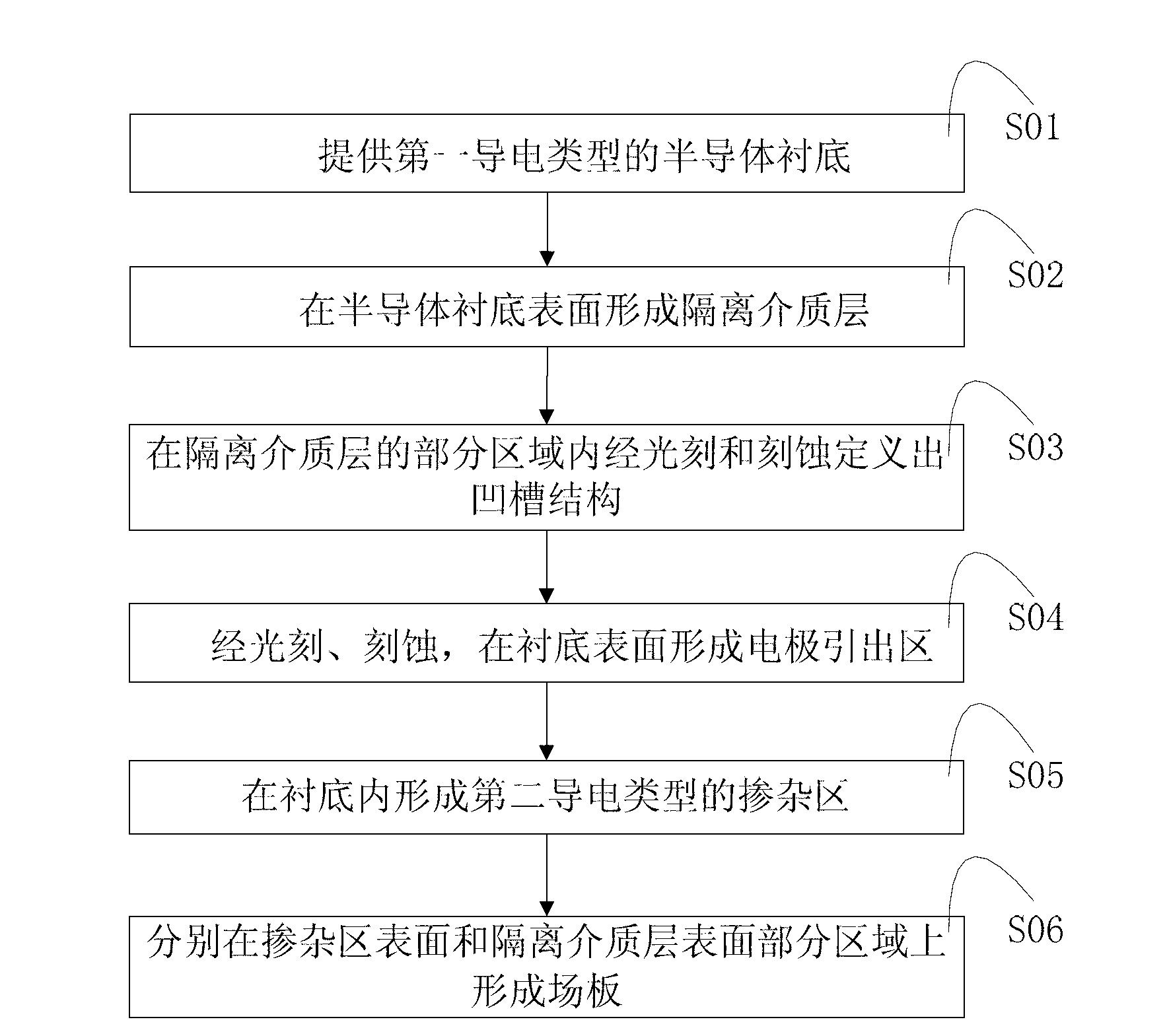
[0028] The terminal structure and manufacturing method of the high-voltage semiconductor device provided by the present invention will be further described in detail below in conjunction with the accompanying drawings and specific embodiments. Advantages and features of the present invention will be apparent from the following description and claims. It should be noted that all the drawings are in a very simplified form and use imprecise scales, and are only used to facilitate and clearly assist the purpose of illustrating the embodiments of the present invention.
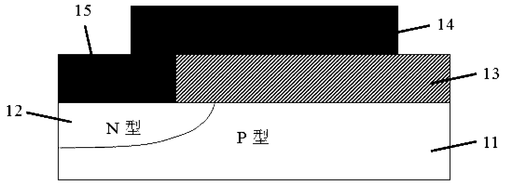
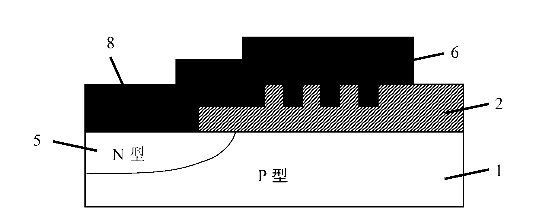
[0029] The invention provides a terminal structure of a high-voltage semiconductor device. see figure 2 , figure 2 It is a structural schematic diagram of a preferred embodiment of a terminal structure of a high-voltage semiconductor device of the present invention. For ease of description, in this embodiment, specific P-type and N-type regions are included, and a P-type silicon substrate 1 is taken as an example, but this is not intended to limit the scope of the present invention. like figure 2 As shown, the terminal structure of the high-voltage semiconductor device in this embodiment includes: a P-type semiconductor substrate 1, an N-type doped region 5 located in the P-type semiconductor substrate, and isolation on the surface part of the P-type semiconductor substrate 1. The dielectric layer 2, and the extraction electrode 8 located on the surface of the N-type doped region 5 and the field plate 6 located on the surface part of the isolation dielectric layer 2, the extraction electrode 8 is connected to the field plate 6, wherein the isolation dielectric layer 2 contains a groove structure covered by a field plate 6. It should be noted that, in the present invention, the field plate material can be but not limited to metal Ti/Al, Ti/TiN/Al, and the thickness of the field plate 6 can be but not limited to 3 μm.
[0030] In the present invention, the semiconductor substrate can be but not limited to semiconductor materials such as silicon, germanium or silicon germanium, and the isolation dielectric layer 2 can be but not limited to silicon dioxide, silicon nitride, hafnium dioxide, zirconium dioxide or other insulating materials. One or more mixtures of dielectric layers. In this embodiment, the semiconductor substrate is a P-type single crystal silicon substrate 1, and the isolation dielectric layer 2 is silicon dioxide. In the present invention, the thickness of the isolation dielectric layer 2 ranges from 0.1 to 3 μm, the depth of the groove is 1/4 to 3/4 of the thickness of the isolation dielectric layer 2, and the ratio of the width to the depth of the groove is 1/2 to 2.
[0031] now attached Figure 3-8 , the method for preparing the terminal structure of the above-mentioned high-voltage semiconductor device in this embodiment of the present invention is further described in detail.
[0032] image 3 It is a process flow chart of a method for preparing a terminal structure of a high-voltage semiconductor device in the above-mentioned preferred embodiment of the present invention.
[0033] Figure 4-8 It is a schematic cross-sectional view of specific preparation steps of a method for preparing a terminal structure of a high-voltage semiconductor device in the above-mentioned preferred embodiment of the present invention. In the present invention, the semiconductor substrate can be, but not limited to, semiconductor materials such as silicon, germanium, or germanium silicon. example, but this is not intended to limit the scope of the present invention.
[0034] see image 3 The specific steps of the preparation method of a terminal structure of a high-voltage semiconductor device in this embodiment are as follows:
[0035] Step S01: providing a P-type silicon substrate 1;
[0036] Step S02: Please refer to Figure 4, using but not limited to chemical vapor deposition to form an isolation dielectric layer 2 on the surface of the P-type silicon substrate 1; the isolation dielectric layer 2 can be but not limited to silicon dioxide, silicon nitride, hafnium dioxide, zirconium dioxide or other insulating One or several mixtures of dielectric layers. In this embodiment, the isolation dielectric layer 2 is silicon dioxide. The thickness of the isolation dielectric layer 2 is in the range of 0.1-3 μm. In this embodiment, the thickness of the isolation dielectric layer 2 may be, but not limited to, 1 μm.
[0037] Step S03: See Figure 5 In a partial area of ​​the isolation dielectric layer 2, a groove structure is formed by photolithography and etching. Concretely, first spin-coat a layer of photoresist 3 on the isolation dielectric layer 2, then form a groove pattern in the photoresist 3 through photolithography, then use the groove pattern on the photoresist 3 as a template but not The method limited to reactive ion etching etches the isolation dielectric layer 2, forms a groove structure in the isolation dielectric layer 2, and removes the glue. In the present invention, the depth of the groove is 1/4-3/4 of the thickness of the isolation medium layer 2, and the ratio of the width to the depth of the groove is 1/2-2. In this embodiment, the width of each groove is 0.5 μm, the depth of the groove is 0.5 μm, and the ratio of width to depth is 1:1.
[0038] Step S04: See Image 6 , through photolithography and etching on the isolation dielectric layer 2, an electrode lead-out region 7 is formed on the surface of the semiconductor substrate 1; specifically, firstly, the photoresist 4 is spin-coated on the isolation dielectric layer 2, and then photoetched on the photoetching layer. A groove pattern is formed in the glue 4, and then the groove pattern on the photoresist 4 is used as a template to etch the isolation dielectric layer 2 by but not limited to a dilute hydrofluoric acid solution, so that the P-type An electrode lead-out area 7 is defined on the surface of the silicon substrate 1, and the glue is removed. In this embodiment, the thickness of the removed isolation dielectric layer 2 may be, but not limited to, 0.5 μm.
[0039] Step S05: See Figure 7 The P-type silicon substrate 1 is doped with N-type impurities, such as phosphorus or arsenic, by ion implantation, but in this embodiment, the impurities can be activated by annealing, so as to control the junction depth and form N-type doped region 5 . It should be noted that the surface of the N-type doped region 5 is the electrode lead-out region 7 .
[0040] Step S06: See Figure 8 , using but not limited to evaporation or sputtering to deposit a metal layer on the surface of the N-type doped region 5 (electrode lead-out region 7) and the surface part of the isolation dielectric layer 2, and then defined by photolithography and etching processes The metal layer is deglued, and an extraction electrode 8 is formed on the surface of the N-type doped region 5, and a field plate 6 is formed on a part of the surface area of ​​the isolation dielectric layer 2, and the extraction electrode 8 is connected to the field plate 6. It should be noted that the groove in the isolation dielectric layer 2 is covered by the field plate 6, the material of the field plate 6 can be but not limited to Ti/Al or Ti/TiN/Al, and the thickness of the metal layer can be but not limited to 3 μm .
[0041] Figure 9 It is a comparison diagram of the electric field intensity on the semiconductor surface between the terminal structure of the present invention and the terminal structure in the prior art. Wherein, the curve 51 represents the distribution curve of the surface electric field intensity of the terminal structure in the prior art, and the curve 52 represents the distribution curve of the surface electric field intensity of the terminal structure of the present invention. Depend on Figure 9 It can be seen that the surface electric field of the terminal structure of the present invention has multiple peaks, and the overall electric field intensity is larger than that of the prior art, so it can bear a higher breakdown voltage.
[0042] Compatible with existing high voltage semiconductor device termination structures such as figure 1 As shown), the terminal structure of the high-voltage semiconductor device of the present invention mainly uses the isolation dielectric layer with a groove structure under the field plate to improve the withstand voltage capability. Due to the existence of the groove, the distance between the field plate and the semiconductor substrate is shortened, the coupling effect between the field plate and the substrate is enhanced, and the electric field intensity in this region is increased. In this way, by setting several groove structures on the isolation dielectric layer below the field plate, the effect of the field plate absorbing the electric force line can be better, and the original PN junction and the two peak electric fields below the outer boundary of the field plate can be made. The electric field strength in the region is generally increased, thereby increasing the breakdown voltage, and the preparation process is simple.
[0043] The above description is only a description of the preferred embodiments of the present invention, and does not limit the scope of the present invention. Any changes and modifications made by those of ordinary skill in the field of the present invention based on the above disclosures shall fall within the protection scope of the claims.

PUM

PropertyMeasurementUnit
Thickness0.1 ~ 3.0µm
Thickness range0.1 ~ 3.0µm

Description & Claims & Application Information

We can also present the details of the Description, Claims and Application information to help users get a comprehensive understanding of the technical details of the patent, such as background art, summary of invention, brief description of drawings, description of embodiments, and other original content. On the other hand, users can also determine the specific scope of protection of the technology through the list of claims; as well as understand the changes in the life cycle of the technology with the presentation of the patent timeline. Login to view more.

Similar technology patents

Facing tooth stepped type magnetofluid sealing device

PendingCN109780218AGood magnetic effectImprove pressure resistance
Owner:GUANGXI UNIVERSITY OF TECHNOLOGY

High-temperature and high-pressure clamp holder and using method thereof

PendingCN114252378Akeep in good touchImprove pressure resistance
Owner:QINGDAO SHIDA HUASONG SCI & TECH

Power supply device, electric appliance and filter circuit

PendingCN110971112AImprove pressure resistanceAvoid filter failure
Owner:GUANGDONG MEIZHI COMPRESSOR

High-pressure-resistant precision aluminum alloy circular tube

PendingCN114473346AImprove reinforcement effectImprove pressure resistance
Owner:ANHUI XIN FA ALUMINUM PROD

Classification and recommendation of technical efficacy words

  • Enhanced coupling
  • Improve pressure resistance

Circuit board and electric connector with same

PendingCN109688698Aenhanced couplingReduce signal crosstalk
Owner:OUPIN ELECTRONICS KUNSHAN

Structure and method for improving double-grating coupling

ActiveCN108878237AIncrease the interaction space of injection wavesenhanced coupling
Owner:UNIV OF ELECTRONIC SCI & TECH OF CHINA

Focusing coupling electrode for hardened site detection

PendingCN112099096Aenhanced couplingReduce ground resistance
Owner:POWERCHINA BEIJING ENG

High-pressure-resistant flat heat pipe and machining method thereof

ActiveCN104713395AImprove pressure resistanceWide operating temperature range
Owner:SHANGHAI INST OF SATELLITE EQUIP
Why Eureka
Try Eureka