
Organic electroluminescent device

An electroluminescent device and luminescence technology, which is applied in the direction of electric solid-state devices, electrical components, semiconductor devices, etc., can solve the problems of poor universality and increased cost, and achieve the effect of improving performance

Inactive Publication Date: 2013-04-03
TAIYUAN UNIV OF TECH
View PDF2 Cites 14 Cited by
  • Summary
  • Abstract
  • Description
  • Claims
  • Application Information

AI Technical Summary

Problems solved by technology

However, these methods have strong selectivity to wavelength. Since OLED emission is mostly broad-spectrum emission, it not only has poor universality, but also increases the cost. In addition, other performances of the device are often sacrificed.

Method used


Image

  • Organic electroluminescent device
  • Organic electroluminescent device
  • Organic electroluminescent device

Examples


Embodiment 1

[0033] The structure of the organic electroluminescent device A1 in this embodiment is:

[0034] A1: ITO / m-MTDATA (20nm) / NPB (50nm) / TCTA (10nm) / TCTA: TPBi: Ir(piq) 2 acac (7wt%, 20nm) / TPBi (20nm) / TPBi: Cs 2 CO 3 (10wt%, 10nm) / C60 (20nm) / CuPc (20nm) / m-MTDATA: F4-TCNQ (20wt%, 10nm) / NPB (40nm) / TCTA (10nm) / TCTA: TPBi: Ir(piq) 2 acac (7wt%, 20nm) / TPBi (30nm) / TPBi: Cs 2 CO 3 (10wt%, 20nm) / Al (100nm).

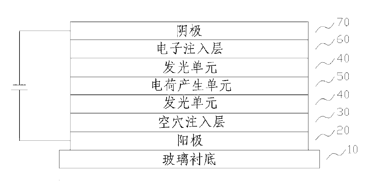
[0035] The structure of the organic electroluminescent device is as follows figure 1 As shown, a series structure is adopted as a whole, consisting of two light-emitting units 40 and a charge generating unit 50. The transparent conductive film ITO deposited on the glass substrate 10 is used as the anode 20 of the device, and Al is used as the cathode 70 of the device. A hole injection layer 30 and an electron injection layer 60 are evaporated respectively after the ITO and before the Al electrode to improve the injection of electrons and holes. T...

Embodiment 2

[0046] At the same time, an organic electroluminescent device B1 comprising a double light-emitting unit and a reference device B2 with a single light-emitting unit were prepared, and its specific structure was as follows:

[0047] B1: ITO / m-MTDATA (20nm) / NPB (50nm) / TCTA (10nm) / TCTA: TPBi: Ir(mdq) 2 acac (7wt%, 20nm) / TPBi (20nm) / TPBi: Cs 2 CO 3 (10wt%, 10nm) / C60 (20nm) / pentacene (20nm) / m-MTDATA: F4-TCNQ (20wt%, 10nm) / NPB (40nm) / TCTA (10nm) / TCTA: TPBi: Ir(mdq) 2 acac (7wt%, 20nm) / TPBi (30nm) / TPBi: Cs 2 CO 3 (10wt%, 20nm) / Al (100nm);

[0048] B2: ITO / m-MTDATA (20nm) / NPB (50nm) / TCTA (10nm) / TCTA: TPBi: Ir(mdq) 2 acac (7wt%, 20nm) / TPBi (30nm) / TPBi: Cs 2 CO 3 (10wt%, 20nm) / Al (100nm).

[0049] In this embodiment, C60 / pentacence is used as the charge generating layer, C60 is used as the charge generating auxiliary layer, and pentacene is used as the light-absorbing active layer. The device luminescent dopant is Ir(mdq) 2 acac. ...

Embodiment 3

[0052] At the same time, an organic electroluminescent device C1 comprising a double light-emitting unit and a reference device C2 with a single light-emitting unit were prepared, and its specific structure was as follows:

[0053] C1: ITO / m-MTDATA (20nm) / NPB (50nm) / TCTA (10nm) / TCTA: TPBi: FIrpic (7wt%, 20nm) / TPBi (20nm) / TPBi: Cs 2 CO 3 (10wt%, 10nm) / PTCDI-C8 (20nm) / Pentacene (20nm) / m-MTDATA: F4-TCNQ (20wt%, 10nm) / NPB (40nm) / TCTA (10nm) / TCTA: TPBi: FIrpic (7wt %, 20nm) / TPBi (30nm) / TPBi: Cs 2 CO 3 (10wt%, 20nm) / Al (100nm);

[0054] C2: ITO / m-MTDATA (20nm) / NPB (50nm) / TCTA (10nm) / TCTA: TPBi: FIrpic (7wt%, 20nm) / TPBi (30nm) / TPBi: Cs 2 CO 3 (10wt%, 20nm) / Al (100nm).

[0055] The charge generating unit of this embodiment adopts PTCDI-C 8 / Pentacene heterojunction, with pentacene as charge generation auxiliary layer, PTCDI-C 8 for the light-absorbing active layer. The light-emitting dopant of the device is FIrpic, a blue phospho...


PUM

PropertyMeasurementUnit
Thicknessaaaaaaaaaa

Abstract

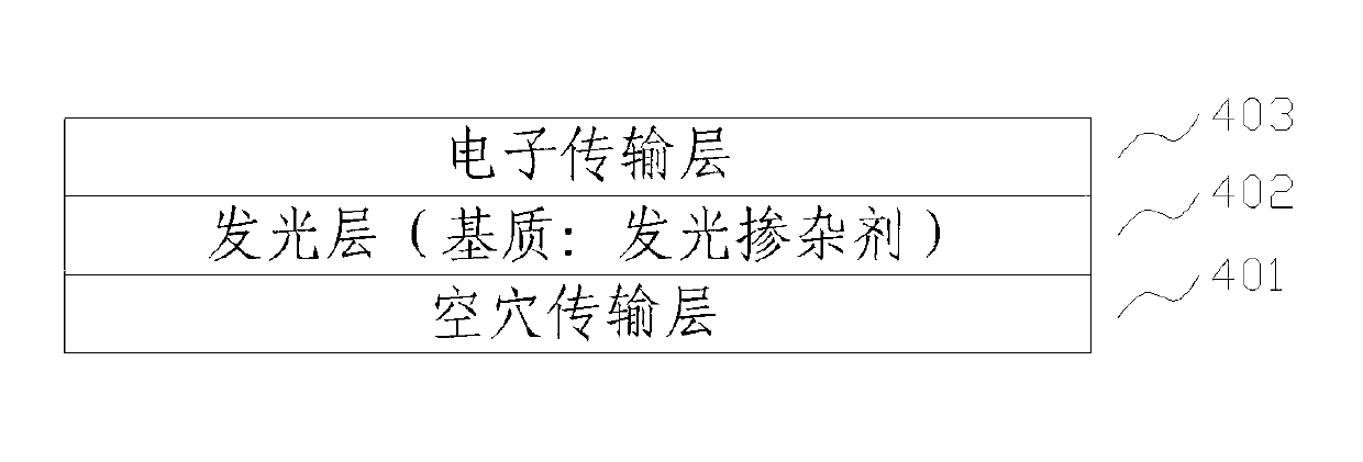
The invention discloses an organic electroluminescent device which comprises electrodes and an organic electroluminescent function layer arranged among the electrodes. The organic electroluminescent function layer comprises at least two luminescent units and an electric charge generating unit arranged among the luminescent units, each luminescent unit comprises a hole transmission layer / matrix and a luminescent layer / electronic transmission layer composed of light emitting dopant according to the direction of outside anode to cathode, the electric charge generating unit comprises an N type doping buffering layer / electric charge generating layer / P type doping buffering layer according to the direction of outside anode to cathode, the electric charge generating layer comprises an electric charge generating assisting layer and a light-absorbing active layer, and overlap between absorption spectrum of the light-absorbing active layer and light emitting spectrum of the light emitting dopant exists. The organic electroluminescent device can effectively utilize optical radiation inside an OLED (organic light emitting diode) to generate electric charge more effectively, and efficient light emitting and slow efficiency reduction are realized.

Description

technical field [0001] The invention belongs to the technical field of organic electroluminescent devices, and relates to an organic electroluminescent device structure that can increase the luminous efficiency of the device and improve the current attenuation of the luminous efficiency by effectively utilizing the internal light radiation of the device. Background technique [0002] Organic electroluminescent technology is based on electro-injection light-emitting technology using organic materials as active layers, and organic electroluminescent devices are also called organic light-emitting devices (organic light-emitting devices, OLEDs). In 1987, Dr. Chine Wan Tang of Kodak Company of the United States successfully used a double-layer sandwich structure similar to the heterogeneous PN junction of inorganic semiconductors to prepare the first electroluminescent device with low driving voltage and high efficiency, which opened the OLED research age. Compared with the curr...

Claims


Application Information

Patent Timeline
IPC IPC(8): H01L51/50
Inventor 刘慧慧颜飞苗艳勤杜晓刚景姝高志翔王华许并社黄维
Owner TAIYUAN UNIV OF TECH
Learn More