
Method for manufacturing multilayer semiconductor ceramic capacitor, and multilayer semiconductor ceramic capacitor

A technology for ceramic capacitors and a manufacturing method, applied in the directions of multilayer capacitors, fixed capacitor dielectrics, capacitors, etc., can solve the problems of high cost, large-scale device, increase in the number of parts, etc., and achieve cost reduction, realization of the number of parts, suppression of The effect of peak voltage

Inactive Publication Date: 2016-01-06
MURATA MFG CO LTD
View PDF7 Cites 0 Cited by
  • Summary
  • Abstract
  • Description
  • Claims
  • Application Information

AI Technical Summary

Problems solved by technology

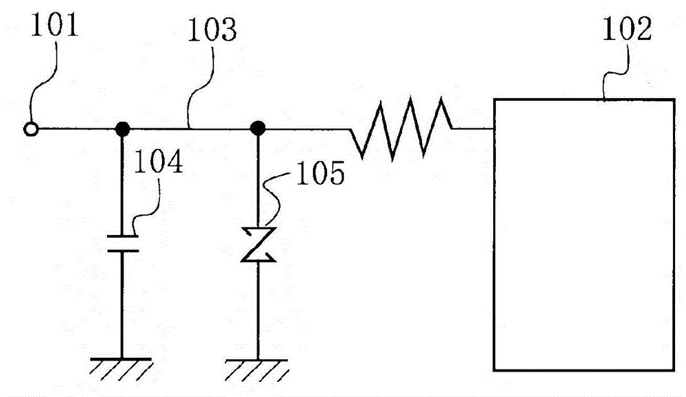
[0009] However, as described above, when the Zener diode 105 is provided in parallel with the bypass capacitor 104, not only the number of parts increases, which leads to high cost, but also the installation space must be secured, which may lead to an increase in the size of the device.

Method used


Image

  • Method for manufacturing multilayer semiconductor ceramic capacitor, and multilayer semiconductor ceramic capacitor
  • Method for manufacturing multilayer semiconductor ceramic capacitor, and multilayer semiconductor ceramic capacitor
  • Method for manufacturing multilayer semiconductor ceramic capacitor, and multilayer semiconductor ceramic capacitor

Examples


Embodiment

[0084] 〔Sample making〕

[0085] Prepare SrCO as the original raw material of ceramics 3 , to prepare a specific surface area of ​​30m 2 / g (average particle size: about 30nm) TiO 2 , and LaCl as the donor compound 3 . In addition, LaCl was weighed so that the content of La was 0.8 mol with respect to 100 mol of Ti element. 3 , and further weigh SrCO so that the mixed molar ratio m (=Sr site / Ti site) of Sr site and Ti site becomes 1.008 3 and TiO 2 .

[0086] Then, with respect to 100 parts by weight of these weighing objects, after adding 3 parts by weight of polycarboxylate ammonium salt as a dispersant, PSZ balls with a diameter of 2 mm and pure water are thrown into a ball mill together as a grinding medium, and 16 parts by weight are carried out in the ball mill. Hours of wet mixing made the slurry.

[0087] Next, after evaporating and drying the slurry, a calcining treatment was performed at a temperature of 1400° C. for 2 hours in the air atmosphere to obtain a c...


PUM

PropertyMeasurementUnit
capacitanceaaaaaaaaaa

Abstract

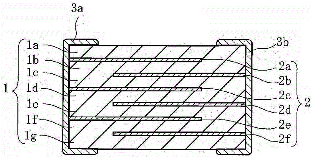
A method of manufacturing a SrTiO3 barrier layer type stacked semiconductor ceramic capacitor comprising: a step of producing calcined powder for producing a calcined powder by performing a calcination process after weighing a given amount of Sr compound, Ti compound and donor compound, and mixing and grinding them; a step of producing heat-treated powder for producing a heat-treated powder by mixing an acceptor compound with the calcined powder and heat-treating the mixture; a step of forming a stacked structure for producing ceramic green sheet by molding the heat-treated powder, and subsequently forming a stacked structure by alternately laminating an internal electrode layer and the ceramic green sheet; and a calcination step of performing a second calcination process under air atmosphere after performing a first calcination process to the stacked structure under reducing atmosphere, wherein the second calcination process is performed under temperature atmosphere of 450°C to 580°C. Hereby, a SrTiO3 barrier layer type stacked semiconductor ceramic capacitor is realized which has good absorption performance for ESD even if electrostatic capacitance has a low value such as 1nF.

Description

technical field [0001] The present invention relates to a method of manufacturing a multilayer semiconductor ceramic capacitor, and a multilayer semiconductor ceramic, and more specifically, relates to a method using SrTiO 3 A method for manufacturing a grain boundary insulation type multilayer semiconductor ceramic capacitor, and a multilayer semiconductor ceramic capacitor manufactured using the manufacturing method. Background technique [0002] With the development of electronic device technology in recent years, portable electronic devices such as mobile phones and notebook computers, and in-vehicle electronic devices mounted on automobiles have spread, and electronic devices have been required to be miniaturized and multifunctional. [0003] On the other hand, in order to achieve miniaturization and multifunctionalization of electronic equipment, a large number of semiconductor elements such as various ICs and LSIs are used, and the noise immunity of electronic equipme...

Claims


Application Information

Patent Timeline
Patent Type & Authority Patents(China)
IPC IPC(8): H01G4/12H01G4/30
CPCH01G4/1227C01G23/003C01G23/006C01P2002/50C04B35/47C04B35/638C04B2235/6025C04B2235/652C04B2235/6582C04B2235/6586C04B2235/661C04B2235/79C04B2237/346C04B2237/68H01G4/12H01G4/30
Inventor 川本光俊
Owner MURATA MFG CO LTD
Learn More