A light-emitting diode epitaxial structure
A technology of light-emitting diodes and epitaxial structures, which is applied to electrical components, circuits, semiconductor devices, etc., can solve the problems of reduced luminous efficiency of materials, less overlapping of electron and hole wave functions, red shift of luminous wavelength, etc. Concentration, the effect of improving the internal quantum luminous efficiency
- Summary
- Abstract
- Description
- Claims
- Application Information
AI Technical Summary
Problems solved by technology
Method used
Image
Examples
Embodiment 1
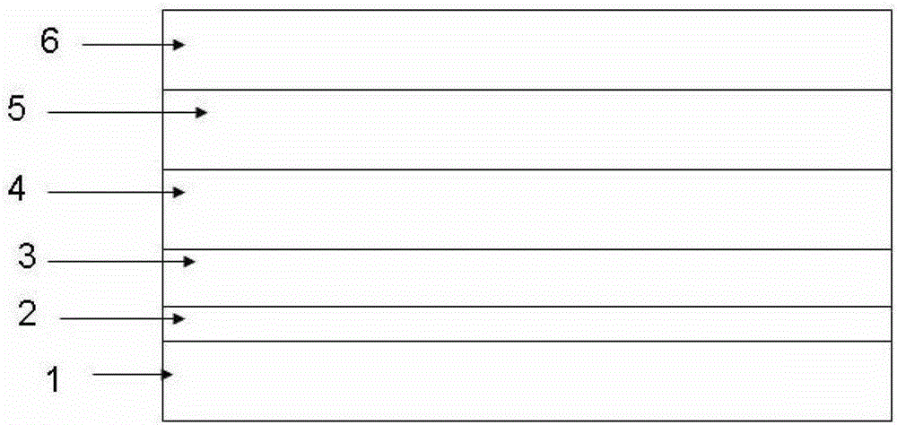
[0053] The LED epitaxial structure is a GaN-based LED epitaxial structure, such as figure 2 As shown, the GaN-based LED epitaxial material structure includes a substrate 1, a nucleation layer 2 sequentially formed on the substrate, an undoped nitride buffer layer 3, an N-type electron injection layer 4, and multiple quantum wells. Source layer 5, and P-type hole injection layer 6.
[0054] Wherein, the substrate 1 includes but not limited to Si substrate, SiC substrate, sapphire substrate.
[0055] Optionally, the material of the nucleation layer 2 is GaN or Al x Ga 1-x N(0≤x≤0.2) composition, or a combination of both.
[0056] Optionally, the material of the undoped nitride buffer layer 3 is GaN, Al x Ga 1-x N, In x Ga 1-x One or more of N, 0≤x≤0.2.
[0057] Optionally, the material of the N-type electron injection layer 4 is N-type doped GaN, Al x Ga 1-x N, In x Ga 1-x One or more of N, 0≤x≤0.2.
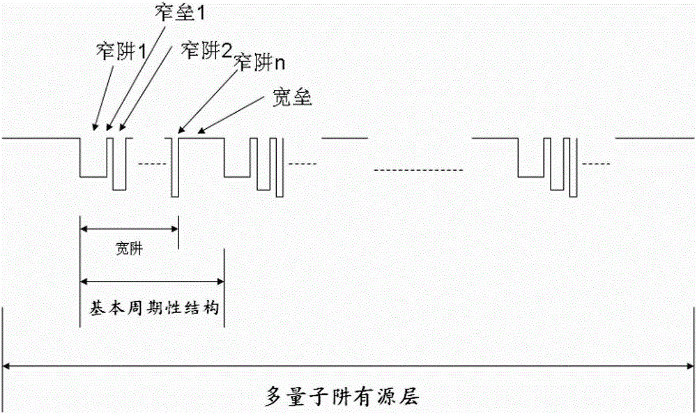
[0058] In this GaN-based LED epitaxial structure, the basic peri...
Embodiment 2
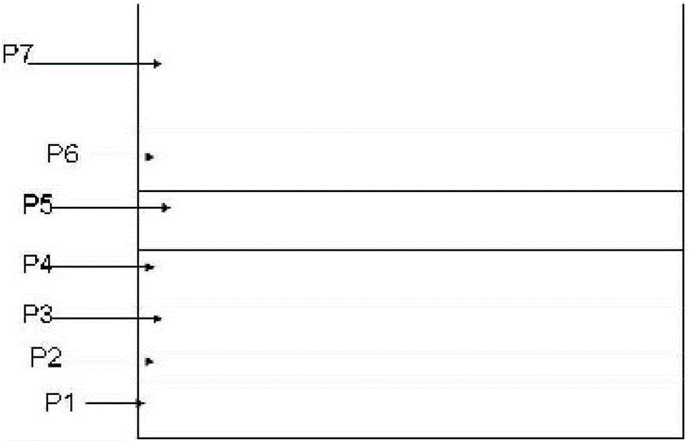
[0074] The LED epitaxial structure is a quaternary AlGaInP-based LED. like image 3 As shown, the quaternary AlGaInP-based LED epitaxial structure includes a substrate P1, a GaAs buffer layer P2 sequentially formed on the substrate, a distributed Bragg reflection layer P3, an N-type electron injection layer P4, and a multi-quantum well active layer. Layer P5, P-type hole injection layer P6, and window layer P7.
[0075] Optionally, the substrate P1 is an N-type GaAs substrate with a thickness of 100-300 microns.
[0076] Optionally, the N-type GaAs buffer layer P2 on the substrate P1 has a doping concentration of 5E17~5E19cm -3 , the thickness is 0.1~0.5 microns.
[0077] Optionally, the distributed Bragg reflection layer P3 is N-type doped Al x Ga 1-x As / Al y Ga 1-y As, where, 0.5≤x≤1, 0.3≤y≤0.7, or (Al x Ga 1-x ) 0.5 In 0.5 P / (Al x1 Ga 1-x1 ) 0.5 In 0.5 P among them, 0.5≤x≤1, 0≤x1≤0.6, x>x1, or different periodic combinations of the above two,
[0078] Option...
PUM
 Abstract
Description
Claims
Application Information


