Preparation method of nitrogen-doped titanium oxide thin film

A technology of titanium dioxide and thin film, which is applied in the field of preparation of nitrogen-doped titanium dioxide thin film, which can solve the problems of low photon quantum efficiency, impossibility of doping state, precise control of component distribution, etc., and achieve the effect of improved utilization rate, remarkable performance and complete film structure

Active Publication Date: 2013-06-19
INST OF MICROELECTRONICS CHINESE ACAD OF SCI
View PDF1 Cites 18 Cited by
  • Summary
  • Abstract
  • Description
  • Claims
  • Application Information

AI Technical Summary

Problems solved by technology

However, N-doped TiO 2 None of the preparation methods can achieve precise control of the doping state, composition distribution and doping amount of N, so that N-doped TiO 2 Post-visible light response photon inefficiency

Method used


Image

  • Preparation method of nitrogen-doped titanium oxide thin film
  • Preparation method of nitrogen-doped titanium oxide thin film
  • Preparation method of nitrogen-doped titanium oxide thin film

Examples


Embodiment 1

[0029] A kind of preparation method of nitrogen-doped titanium dioxide film provided by the present invention comprises:

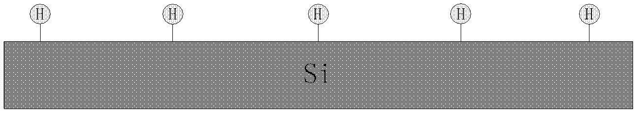
[0030] Step S1: if figure 1 As shown, the silicon-hydrogen bond is formed on the surface of the silicon wafer substrate by treating the surface of the silicon wafer substrate with standard solution and hydrofluoric acid. The standard solution used in this example is prepared by boiling sulfuric acid and hydrogen peroxide at a ratio of 5:100 for 5 minutes.

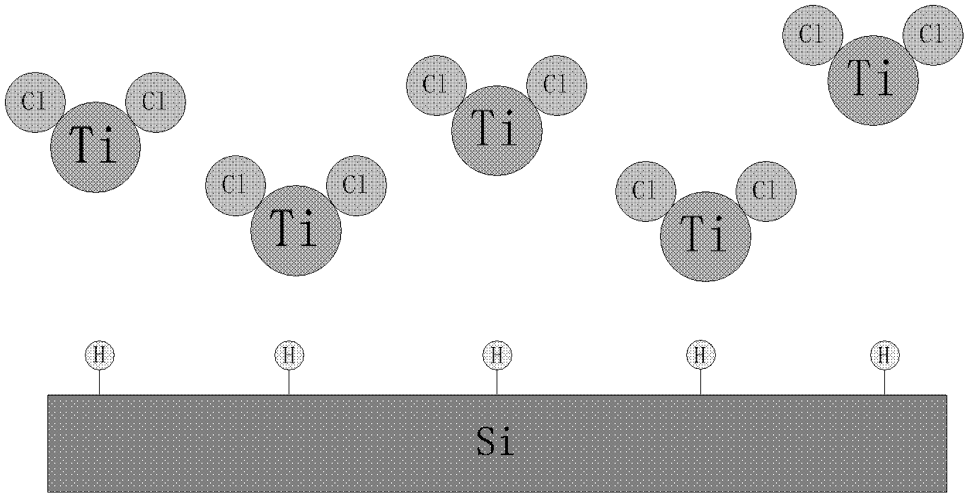
[0031] Step S2: placing the hydrogenated silicon wafer substrate in the reaction chamber of the atomic layer deposition equipment.

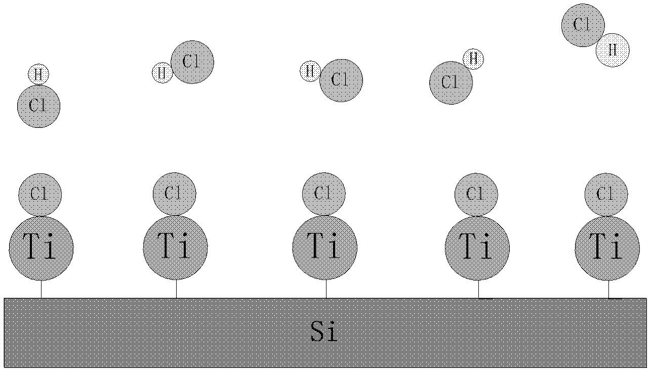
[0032] Step S3: Turn on the device, adjust the working parameters, and achieve the required working conditions for the experiment. combine figure 2 , image 3 As shown, the titanium-containing source gas is introduced into the reaction chamber of the plasma atomic layer deposition equipment, and the titanium atoms in the titanium-containing source gas are adsorbed on ...

Embodiment 2

[0037] The difference between this embodiment and Embodiment 1 is that when nitrogen is used as the carrier gas to transport hydrogen gas into the reaction chamber of the atomic layer deposition equipment, the flow rate of nitrogen gas is 1 sccm, the intake time is 0.1s, the reaction time is 1s, and the cleaning time is 1sccm. for 5s, and the substrate temperature is 100°C. The hydrogen flow rate is 1sccm, the plasma discharge power is 1W, and the discharge time is 1s. Other places are completely consistent with Embodiment 1.

Embodiment 3

[0039] The difference between this embodiment and Embodiment 1 is that when nitrogen is used as the carrier gas to transport hydrogen gas into the reaction chamber of the atomic layer deposition equipment, the flow rate of nitrogen gas is 100 sccm, the intake time is 10 s, the reaction time is 10 s, and the cleaning time is 60s, the substrate temperature is 500°C. The hydrogen flow rate is 100sccm, the plasma discharge power is 300W, and the discharge time is 10s. Other places are completely consistent with Embodiment 1.


PUM


Abstract

The invention discloses a preparation method of nitrogen-doped titanium oxide thin film. The method comprises successively introducing titanium-containing gas into a reaction cavity to form silicon-titanium bonds; introducing nitrogen and hydrogen into an atomic layer deposition reaction chamber for plasma discharge, wherein part of nitrogen atoms generated by ionizing the nitrogen form covalent bonds with part of titanium atoms, and non-bonded electrons of the nitrogen atoms bond with ionized hydrogen atoms; introducing an oxygen-containing source into the atomic layer deposition reaction chamber to form titanium-oxygen bonds; and growing layer by layer the titanium oxide thin film containing the nitrogen atoms. The preparation method of the nitrogen-doped titanium oxide thin film provided by the invention utilizes a plasma atomic layer deposition device to dope nitrogen for the titanium dioxide thin film. By utilizing characteristics of monolayer cycle growth of atomic layer deposition and high chemical reactivity of the plasma, the titanium dioxide thin film can be uniformly doped with the nitrogen atoms in the whole thin film structure during a growth process, so that the doped thin film structure is complete, and significant in performance, and can effectively improve utilization rate of TiO2 for visible light.

Description

technical field [0001] The invention relates to the technical fields of atomic layer deposition technology and titanium dioxide doping modification, in particular to a method for preparing a nitrogen-doped titanium dioxide thin film. Background technique [0002] Semiconductor photocatalytic materials have broad application prospects in solving energy and environmental problems. Semiconductor Nano TiO 2 It has become an ideal material for solving energy and environmental problems because of its stable chemical properties, non-toxicity and ability to effectively remove pollutants in the atmosphere and water. However, TiO 2 The forbidden band width of TiO is relatively large (Eg=3.2eV), and the photocatalytic reaction can only occur under ultraviolet light with a wavelength less than 387nm, which means that TiO 2 Can only utilize a small amount of part (about 5%) in sunlight, and the visible light (about 45%) that accounts for the majority in sunlight can't utilize. Doping...

Claims


Application Information

Patent Timeline
Patent Type & Authority Applications(China)
IPC IPC(8): C23C16/30C23C16/50
Inventor 万军赵柯杰黄成强饶志鹏陈波李超波夏洋吕树玲石莎莉
Owner INST OF MICROELECTRONICS CHINESE ACAD OF SCI
Why Eureka
Try Eureka