Insulated gate transistor device and manufacturing technology method thereof

A technology of insulated gate transistors and manufacturing processes, which is applied in the field of electronics to achieve the effects of reducing manufacturing costs, preventing the occurrence of latch-up effects, and facilitating the control of etching processes

Active Publication Date: 2013-06-19
SHANGHAI HUAHONG GRACE SEMICON MFG CORP
View PDF7 Cites 6 Cited by
  • Summary
  • Abstract
  • Description
  • Claims
  • Application Information

AI Technical Summary

Problems solved by technology

The limitation of this process is that the contact holes on the metal buried layer and the contact holes on the N+ need to be formed at the same time, that is to say, when the contact holes are etched, a part of the contact holes need to be etched to...

Method used


Image

  • Insulated gate transistor device and manufacturing technology method thereof
  • Insulated gate transistor device and manufacturing technology method thereof
  • Insulated gate transistor device and manufacturing technology method thereof

Examples


Embodiment Construction

[0031] The present invention will be described in further detail below in conjunction with the accompanying drawings and embodiments.

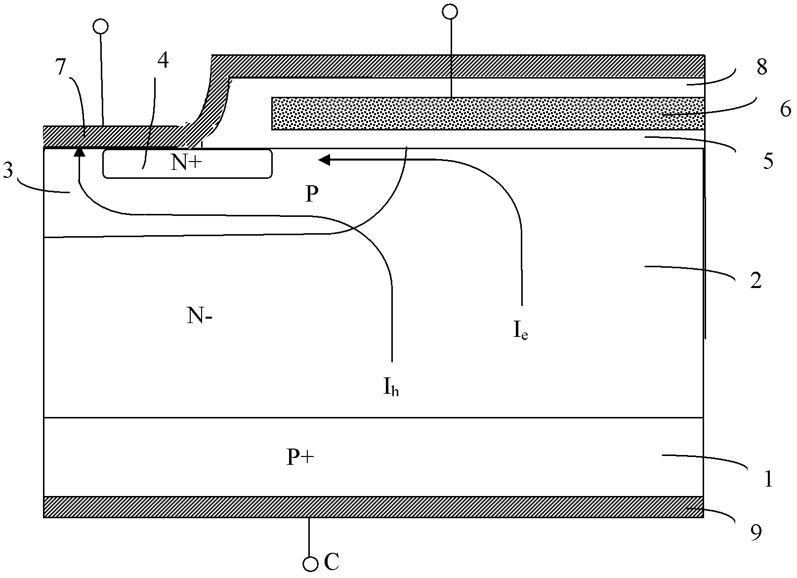
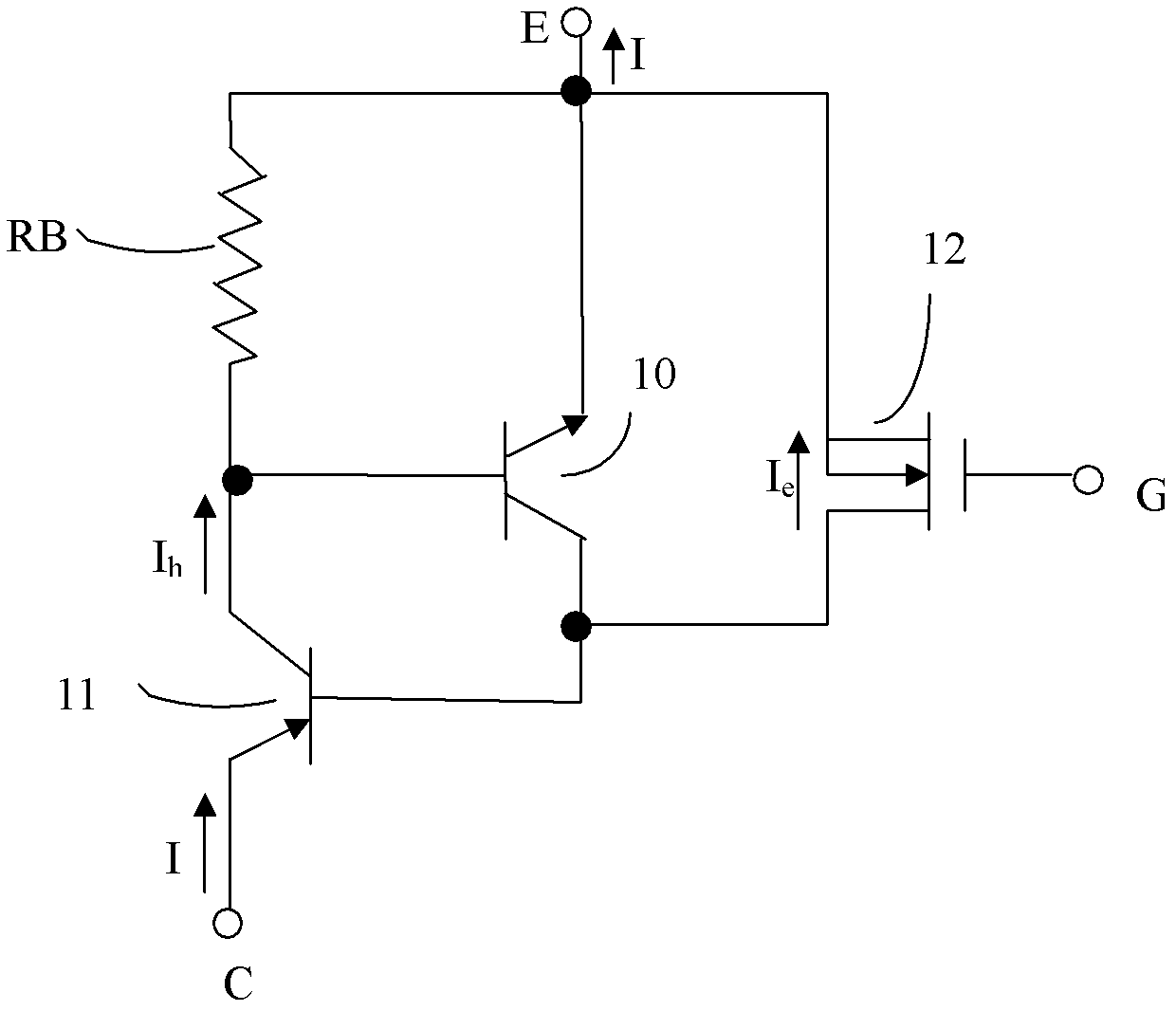
[0032] As shown in Figure 5, the present invention provides a manufacturing process method of an insulated gate transistor device (IGBT), comprising the following steps:

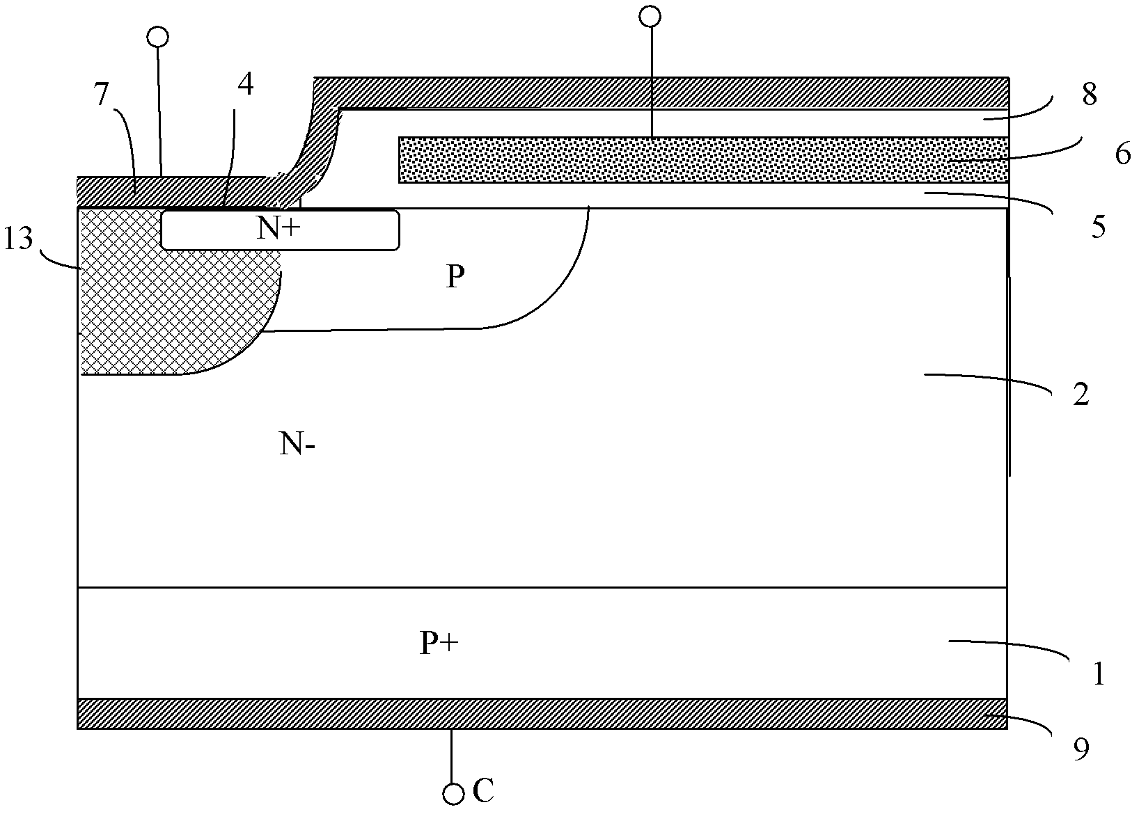
[0033] 1. If Figure 5A As shown, a layer of 50-110um (micrometer) thick N-type epitaxial layer 22 is grown on the surface layer of the P+ semiconductor substrate 21. Then a layer of silicon oxide is grown on the surface of the N-type epitaxial layer 22, and photolithography and etching A mask layer 33 with a certain pattern is formed by the process, and finally P-type impurities such as boron ions are selectively implanted through the mask layer 33 . Then, the implanted ions are diffused and advanced through a high-temperature thermal process to form the first layer of P-type region 23b on the surface.

[0034] 2. If Figure 5B As shown, the mask layer 33 is removed, and...


PUM

PropertyMeasurementUnit
Thicknessaaaaaaaaaa

Abstract

The invention discloses an insulated gate transistor device and manufacturing technology method of the insulated gate transistor device. High-energy ions are filled into a P well region and an interface position of an N+ emitting electrode to from a layer of metal silicide. An ion mixing zone with high condensation is formed in a zone, connected with the emitting electrode, of a partial zone of the N+ emitting electrode (above the buried layer of the metal silicide) in a manner of filling the high-energy ions to accelerate instant heating processing. Thus, a low-resistance zone is formed and the buried layer of metal silicide and a superficial emitting electrode are connected. Compared with traditional technology, according to the manufacturing technology method of the insulated gate transistor device, machining technology of the insulated gate transistor device is simple, manufacturing cost is low, massive production of IGBT products is benefited. The IGBT devices with specific structures can effectively prevent latch-up from happening.

Description

technical field [0001] The invention belongs to the field of electronic technology, relates to a power semiconductor device, in particular to an insulated gate transistor device (IGBT) and a manufacturing process thereof for preventing the latch effect of the insulated gate transistor. Background technique [0002] Insulated Gate Transistor (hereinafter referred to as IGBT) is a new type of power semiconductor device with rapid development and wide application. [0003] like figure 1 As shown, the device structure of a traditional N-type IGBT includes a P+ semiconductor substrate 1, a layer of N- epitaxial layer 2 is grown on the P+ semiconductor substrate 1 by epitaxy, and then a P well region 3 and a P well region 3 are formed by ion implantation. N+ emitter 4. Next, a gate oxide layer 5 and polysilicon 6 are grown in the P well region 3 between the N+ emitter 4 and the N- epitaxial layer 2 as the gate of the field effect transistor, and the gate oxide layer 5 and polysi...

Claims


Application Information

Patent Timeline
IPC IPC(8): H01L21/331H01L21/265H01L29/739
Inventor 刘远良
Owner SHANGHAI HUAHONG GRACE SEMICON MFG CORP
Why Eureka
Try Eureka