
Undoped efficient white organic emitting device and preparation method thereof

An electroluminescent device, non-doping technology, applied in the direction of electric solid-state devices, semiconductor/solid-state device manufacturing, electrical components, etc., can solve the problems of inaccurate concentration control, unstable co-evaporation rate, low luminous efficiency, etc., to achieve No angle dependence, improved device luminous efficiency, and good repeatability

Inactive Publication Date: 2013-06-19
OCEANS KING LIGHTING SCI&TECH CO LTD +1
View PDF4 Cites 8 Cited by
  • Summary
  • Abstract
  • Description
  • Claims
  • Application Information

AI Technical Summary

Problems solved by technology

However, this structure involves multi-component co-evaporation. Due to the distance between the substrate and each evaporation source, the film thickness monitor cannot accurately control the concentration of each component during co-evaporation, the co-evaporation rate is unstable, the repeatability is not good, and It will lead to poor color rendering and low luminous efficiency

Method used

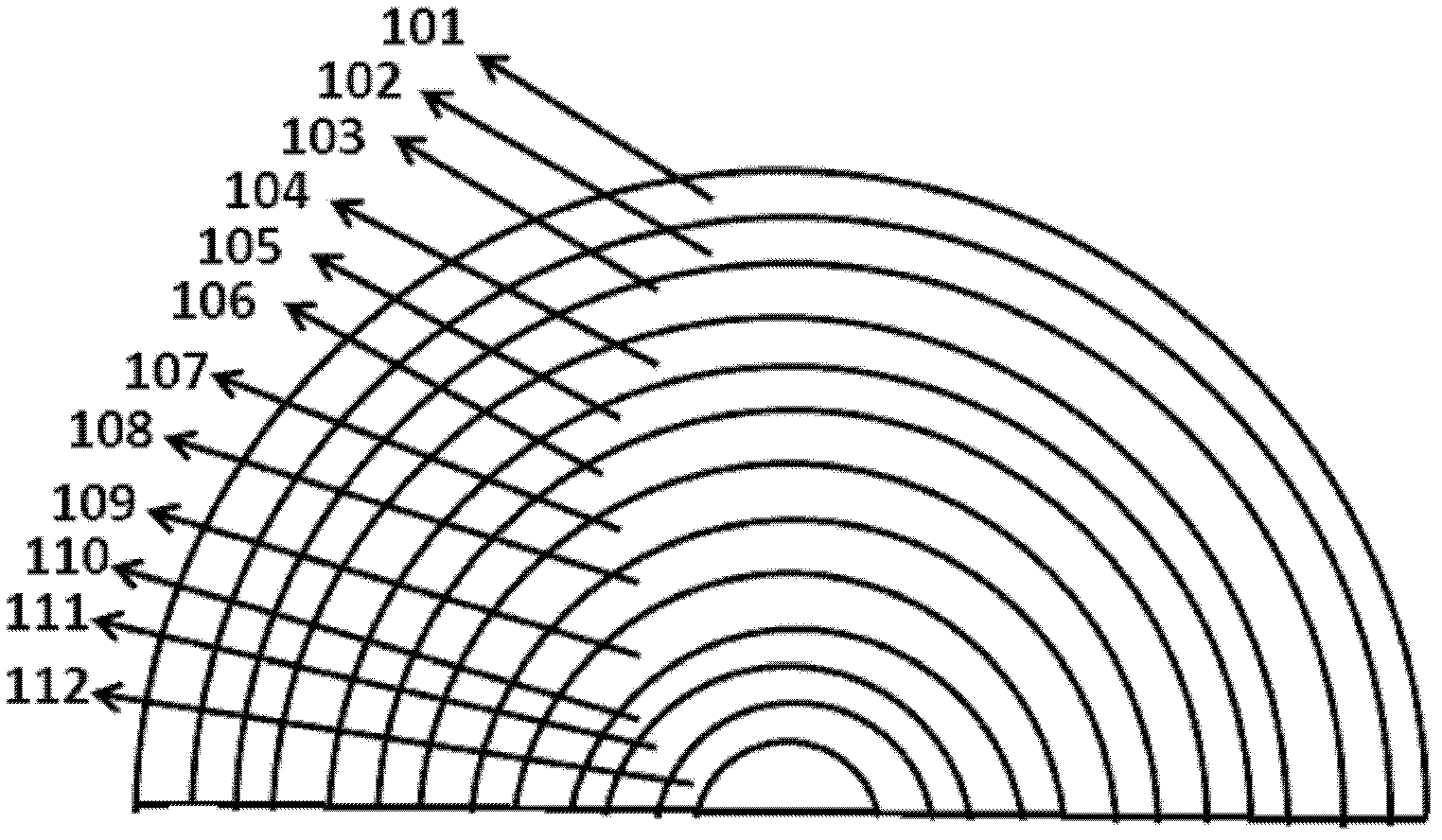

Image

  • Undoped efficient white organic emitting device and preparation method thereof
  • Undoped efficient white organic emitting device and preparation method thereof
  • Undoped efficient white organic emitting device and preparation method thereof

Examples


preparation example Construction

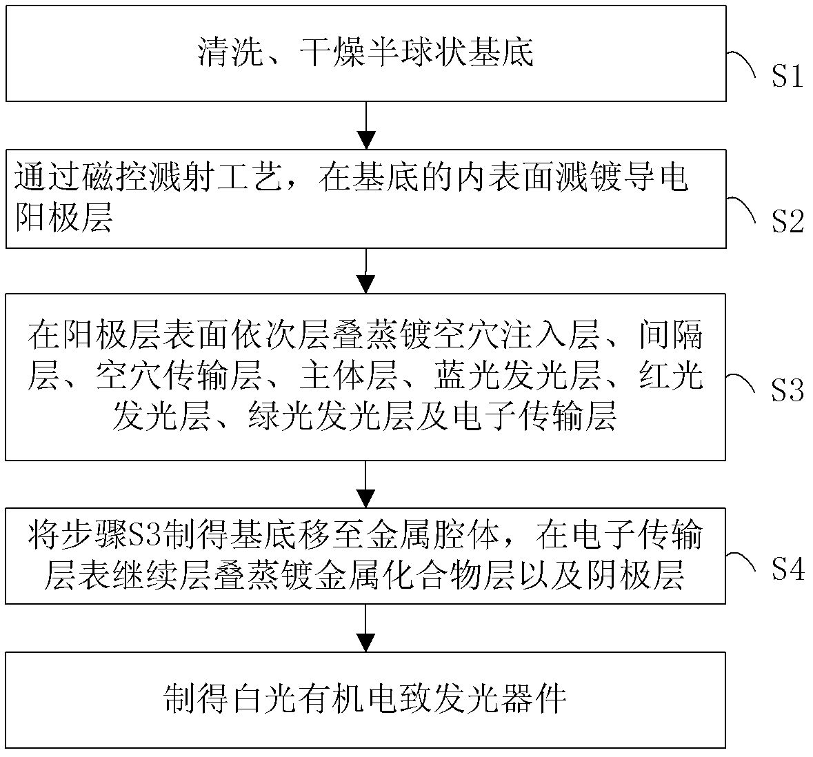
[0044] The preparation method of the above-mentioned non-doped high-efficiency white light organic electroluminescent device, such as figure 2 shown, including the following steps:

[0045] S1. The hemispherical substrate (eg, glass) is ultrasonically cleaned with purified water, acetone, ethanol, etc. for 15 minutes in sequence, and dried after cleaning;

[0046] S2, using the magnetron sputtering process, putting the hemispherical shell-shaped substrate into the vacuum chamber of the magnetron sputtering equipment, and sputtering an anode layer with a thickness of 150 nm on the inner surface of the hemispherical shell-shaped substrate; making the hemispherical shell shaped anode substrate, and then the anode layer was treated with oxygen plasma with a power of 10W for 15min;

[0047] S3. Put the hemispherical shell-shaped anode substrate into the organic vacuum cavity of the evaporation equipment, the hole injection layer, the spacer layer, the hole transport layer, the ma...

Embodiment 1

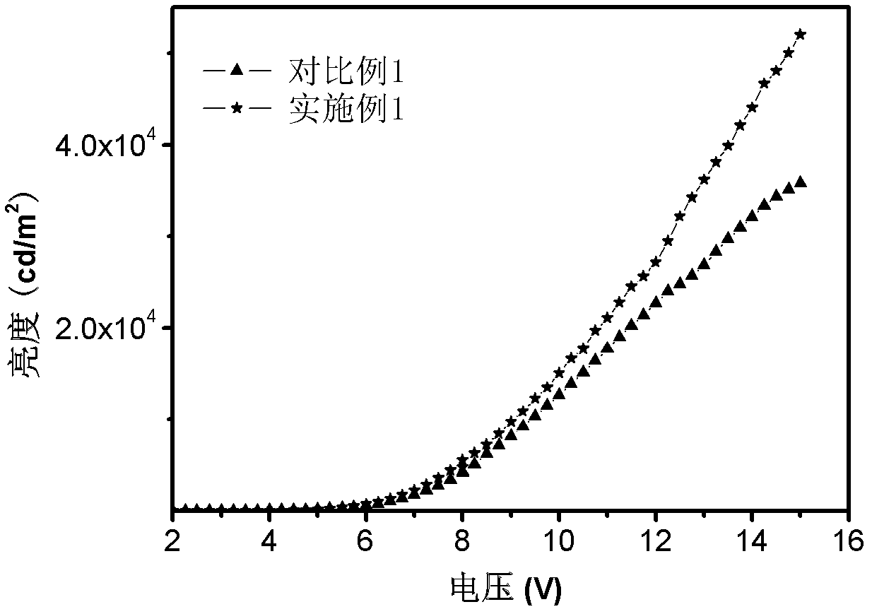
[0054] The hemispherical glass substrate with an inner radius of 5mm and a thickness of 4mm was ultrasonically cleaned with pure water, acetone, ethanol, etc. for 15 minutes in sequence. After cleaning, it was placed in a magnetron sputtering vacuum chamber, and a layer of 150nm thick The ITO. Then put the ITO hemispherical glass into the organic vacuum cavity, and sequentially evaporate the hole injection layer (the material is m-MTDATA, the thickness is 20nm), the spacer layer (the material is HAT, the thickness is 3nm), the hole transport layer (the material is It is TPD, the thickness is 20nm), the main body layer (the material is TCTA, the thickness is 15nm), the blue light emitting layer (the material is Firpic, the thickness is 1nm), the red light emitting layer (the material is Ir(piq) 3 , thickness is 0.3nm), green light emitting layer (material is Ir(ppy) 3 , thickness is 0.5nm), electron transport layer (material is Bphen, thickness is 40nm), and then the substrate...

Embodiment 2

[0056] A hemispherical glass substrate with an inner radius of 3 mm and a thickness of 3 mm was ultrasonically cleaned with pure water, acetone, ethanol, etc. for 15 minutes in sequence. AZO. Then put the AZO hemispherical glass into the organic vacuum cavity, and sequentially evaporate the hole injection layer (the material is m-MTDATA, the thickness is 30nm), the spacer layer (the material is F4-TCNQ, the thickness is 1nm), and the hole transport layer (the material is TCTA, the thickness is 20nm), the main body layer (the material is TCTA, the thickness is 10nm), the blue light emitting layer (the material is Firpic, the thickness is 0.5nm), the red light emitting layer (the material is Ir(piq) 3 , thickness is 0.1nm), green light emitting layer (material is Ir(ppy) 3 , thickness is 0.2nm), electron transport layer (material is Bphen, thickness is 20nm), and then the substrate is moved into the metal chamber, continue to evaporate metal compound layer (material is Cs 2 CO...


PUM


Abstract

The invention belongs to the field of photoelectric devices, and discloses an undoped efficient white organic emitting device and a preparation method thereof. The undoped efficient white organic emitting device comprises a hemispherical shell-shaped base, wherein a positive pole layer, a hole injection layer, a spacer layer, a hole transfer layer, a main body layer, a blue light luminous layer, a red light luminous layer, a green light luminous layer, an electron transfer layer, a metallic compound layer and a negative pole layer are stacked on the inner surface of the hemispherical shell-shaped base in sequence. Due to the fact that the undoped efficient white organic emitting device is hemispherical, total internal reflection loss caused by the difference between the refractive index of the luminous layers and the refractive index of the air is refracted out through a curved surface, loss caused by the lateral waves of an organic layer can be captured, and thus luminous efficiency is improved greatly.

Description

technical field [0001] The invention relates to the field of optoelectronic devices, in particular to a non-doped high-efficiency white light organic electroluminescent device and a preparation method thereof. Background technique [0002] In 1987, Tang and VanSlyke of Eastman Kodak Company in the United States reported a breakthrough in the research of organic electroluminescence. For the first time, they used the vacuum evaporation technology to combine the aromatic diamine with hole transport property and the 8-hydroxyquinoline aluminum (Alq) with high fluorescence efficiency and electron transport property. 3 ) combined to prepare a double-layer organic electroluminescent device. Under the driving voltage of 10V, the device emits green light with a brightness of up to 1000cd / m 2 , the efficiency reaches 1.5lm / W, and the life span exceeds 1000 hours. This milestone work has made people see a bright prospect for the practical and commercialization of organic electrolumi...

Claims


Application Information

Patent Timeline
Patent Type & Authority Applications(China)
IPC IPC(8): H01L51/50H01L51/52H01L51/56
Inventor 周明杰王平
Owner OCEANS KING LIGHTING SCI&TECH CO LTD
Learn More