Preparation method for groove semiconductor discrete device

A discrete device and semiconductor technology, applied in semiconductor/solid-state device manufacturing, electrical components, circuits, etc., can solve the problems of complex steps, poor terminal structure of semiconductor devices, and difficult to generate, so as to reduce manufacturing costs and increase performance prices. the effect of

Inactive Publication Date: 2013-07-03
立新半导体有限公司
View PDF4 Cites 2 Cited by
  • Summary
  • Abstract
  • Description
  • Claims
  • Application Information

AI Technical Summary

Problems solved by technology

[0005] In the existing field of design and manufacture of trench power MOSFETs, the base region and source region of the MOSFET need to be introduced by the steps of base region mask and source region mask respectively, and some previously proposed, such as disclosed U.S. patent documents US07799642, US20090085074, US20110233666, US20110233667, etc., attempt to omit the manufacturing method of the mask step of the base region or the source region. The breakdown voltage and reliability are also relatively poor

Method used


Image

  • Preparation method for groove semiconductor discrete device
  • Preparation method for groove semiconductor discrete device
  • Preparation method for groove semiconductor discrete device

Examples


Embodiment 1

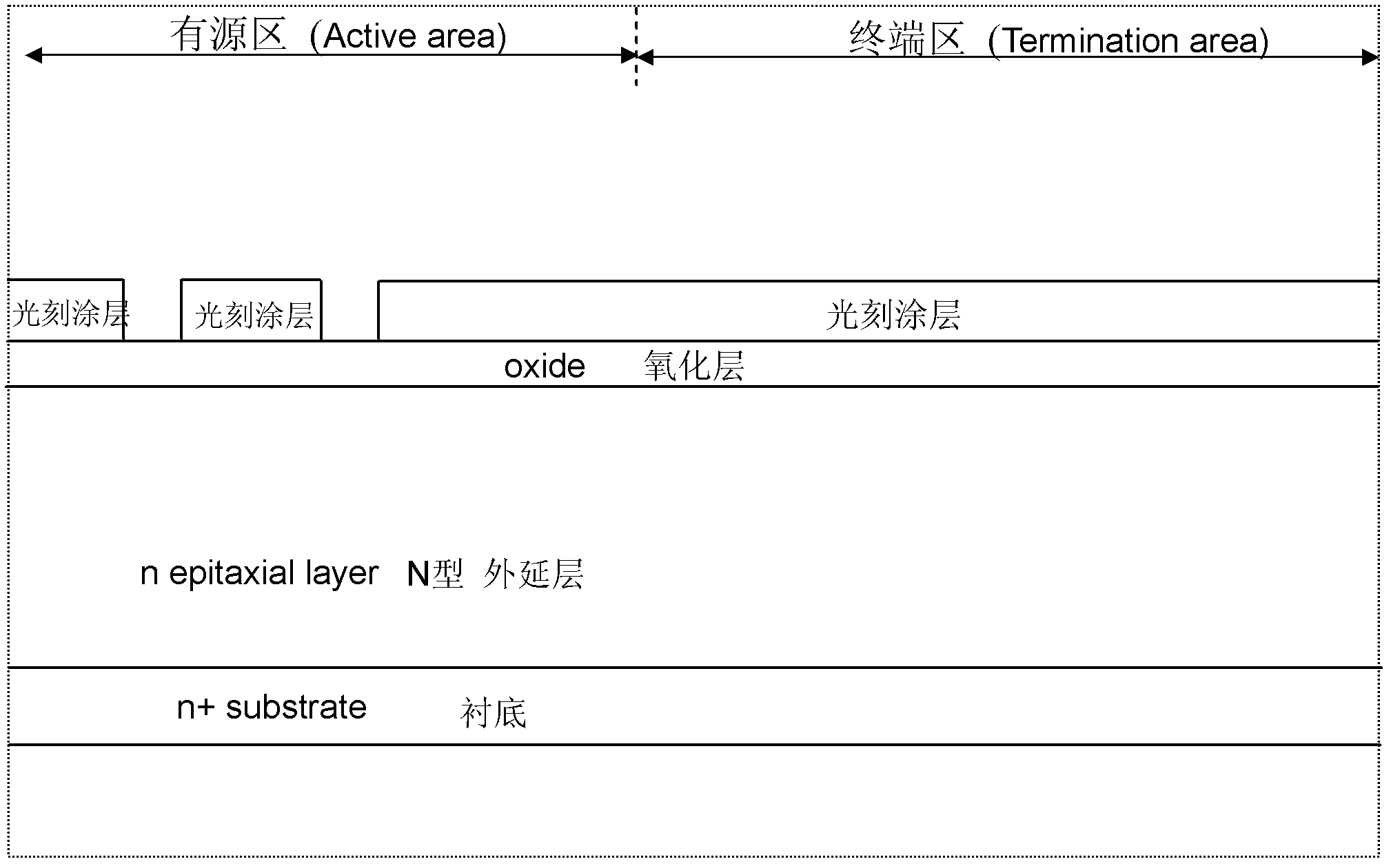
[0068] Such as figure 1 As shown, the epitaxial layer is placed above the substrate. First, an oxide layer (a hard oxide mask with a thickness of 0.3um to 1.5um) is formed on the epitaxial layer by deposition or thermal growth, and then a layer of oxide is deposited on the oxide layer. A photolithographic coating is then patterned through a trench mask to expose portions of the oxide layer.

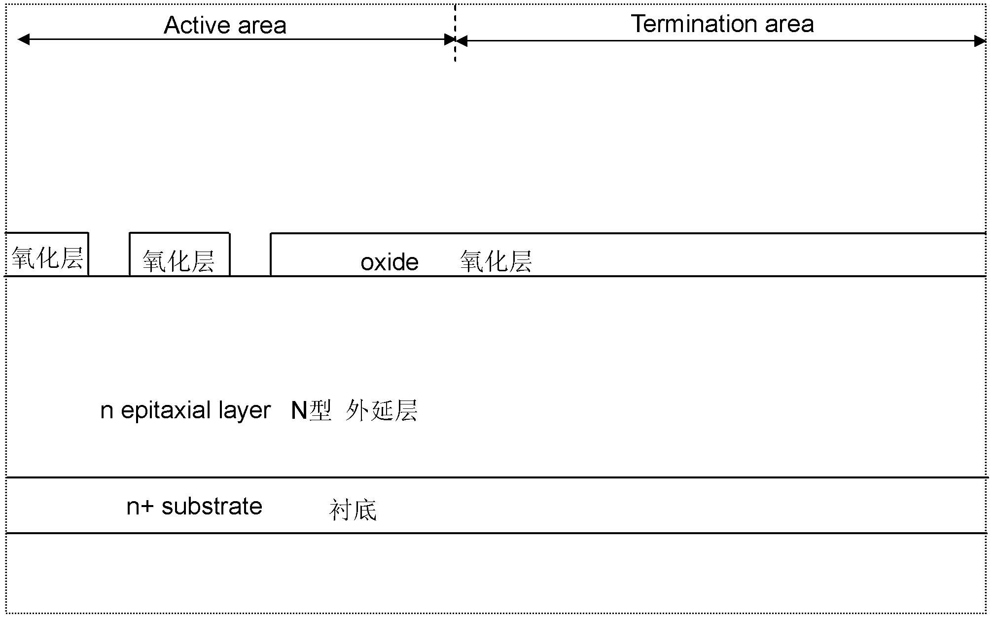
[0069] Such as figure 2 As shown, after dry etching the oxide layer exposed by patterning the trench mask, the epitaxial layer is exposed, and then the photolithographic coating is removed.

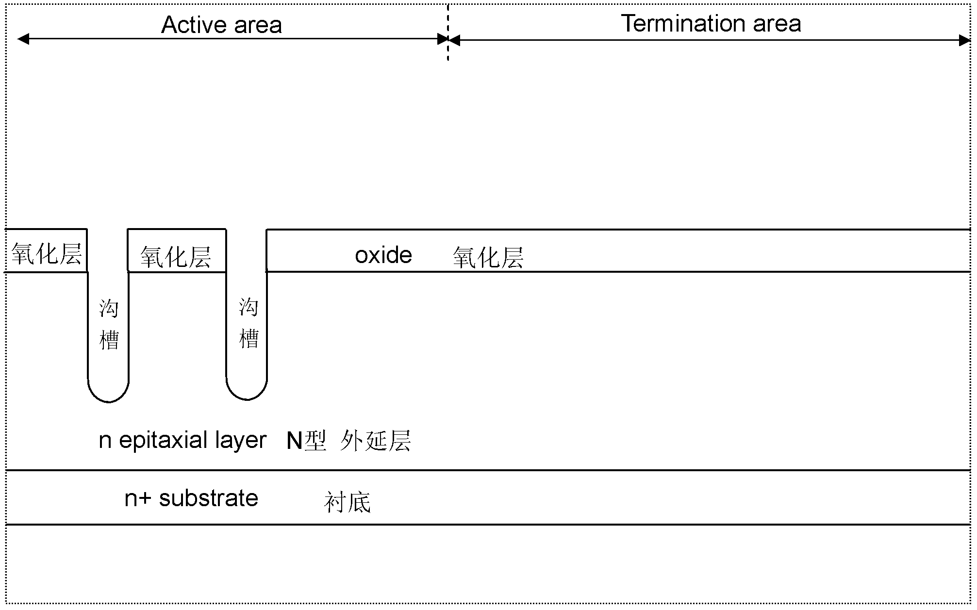
[0070] Such as image 3 As shown, a trench (1.0um to 7.0um in depth and 0.2um to 2.0um in width) is formed by etching, and the trench extends to the N-type epitaxial layer.

[0071] Such as Figure 4 As shown, after the trench is formed, the trench is sacrificially oxidized (10 minutes to 100 minutes at a temperature of 1000° C. to 1200° C.) to eliminate the silicon layer damaged by the plasma d...

Embodiment 2

[0088] It is an embodiment of the present invention.

[0089] Step and embodiment 1 are by Figure 1 to Figure 17 same, then:

[0090] Such as Figure 20 As shown, a layer of LPCVD oxide layer is deposited.

[0091] Such as Figure 21 As shown, the oxide layer is then dry-etched to remove the oxide layer on the opening and expose the epitaxial layer on the opening of the interlayer dielectric.

[0092] Such as Figure 22 As shown, the epitaxial layer containing the dopant is etched through the opening of the interlayer dielectric, so that the contact hole trench (0.4um to 1.0um in depth and 0.2um to 1.2um in width) passes through the N-type source region Enter the P-type base region, and then inject a P-type high dopant into the contact hole trench (dopant concentration is 10 14 up to 5×10 15 / cm 3 ) to reduce the contact resistance between the P-type base region and the metal plug, which effectively increases the safe use area of ​​the device. Such as Figure 23 As ...

Embodiment 3

[0095] It is a variant of the present invention.

[0096] Step and embodiment 1 are by Figure 1 to Figure 17 same, then:

[0097] Such as Figure 24 As shown, a layer of LPCVD oxide layer is deposited, and the opening width of the contact hole mask in the interlayer dielectric is sealed from 0.2um to 0.6um. The width of the sealed opening can be 0.2um, or 0.3um um or 0.4um or 0.5um or 0.6um, depending on the preparation method, and then dry-etch the oxide layer to remove the oxide layer in the unsealed interlayer dielectric openings, exposing the Epitaxial layer: Etching the epitaxial layer containing dopants through opening holes in the interlayer dielectric, so that the contact hole trench (0.4um to 1.0um in depth and 0.2um to 1.0um in width) passes through the N-type source region Enter the P-type base region, and then inject a P-type high dopant into the contact hole trench (dopant concentration is 10 14 up to 5×10 15 / cm 3 ) to reduce the contact resistance between...


PUM


Abstract

The invention discloses a preparation method for a groove semiconductor discrete device. The preparation method for the groove semiconductor discrete device includes the following steps: firstly, eroding an epitaxial layer by utilization of a groove mask to form a plurality of grid electrode grooves; then depositing interlayer medium on the surface of the epitaxial layer, eroding the interlayer medium by utilization of a contact hole mask, open holes are formed in the interlayer medium, injecting p-type and n-type dopant to respectively form a p-type base area and a n-type source area, eroding the surface of the epitaxial layer to form contact grooves, and filling the contact grooves through metal inserting plugs; and finally, depositing a metal layer on the upper surface of the device, and performing metal erosion by utilization of a metal mask to form a metal padding layer and connecting lines. By adoption of the preparation method, the preparation processes of a base area mask and a source area mask are omitted, and manufacturing cost of the device is enabled to be reduced greatly; and meanwhile, original electric properties and reliability of the device can not be affected, and therefore the performance/cost ratio of the device is increased.

Description

technical field [0001] The invention relates to the technical field of semiconductor discrete devices, in particular to a method for preparing a trench semiconductor power discrete device. Background technique [0002] At present, the power MOSFET (Metal Oxide Semiconductor Field Effect Transistor, Metal Oxide Semiconductor Field Effect Transistor) has been widely used in various electronic and communication products, and at the same time, it also has various applications in industry. [0003] Power semiconductor devices represented by power MOSFETs can effectively control high-frequency large currents due to their low on-resistance and high-speed switching. At the same time, power MOSFETs are being widely used as small power conversion components such as power amplifiers, power converters, low noise amplifiers, and some personal computer power supply switches and power circuits, which are characterized by low power consumption and high speed. [0004] Trench power MOSFETs ...

Claims


Application Information

Patent Timeline
Patent Type & Authority Applications(China)
IPC IPC(8): H01L21/336
Inventor 苏冠创
Owner 立新半导体有限公司
Why Eureka
Try Eureka