Method for testing indium content in epitaxial layer of InGaN chip

A technology of element content and test method, applied in the direction of color/spectral characteristic measurement, etc., can solve problems such as difficulty in wafer sample processing

Inactive Publication Date: 2013-07-10
NO 53 RES INST OF CHINA NORTH IND GRP
View PDF2 Cites 0 Cited by
  • Summary
  • Abstract
  • Description
  • Claims
  • Application Information

AI Technical Summary

Problems solved by technology

Because InGaN materials are resistant to acid and alkali solutions, it is very difficult to handle wafer samples. There is no report on the chemical analysis of the content of indium in the epitaxial layer of InGaN wafers.

Method used


Image

  • Method for testing indium content in epitaxial layer of InGaN chip
  • Method for testing indium content in epitaxial layer of InGaN chip

Examples


Embodiment 1

[0031] (1) Sample pretreatment

[0032] Take a 10mm×10mm square InGaN (In 0.12 Ga 0.88 N) Wafer, soak the sample with dilute hydrochloric acid for 10 minutes, rinse it with deionized water, soak it with analytical grade acetone for 5 minutes, and accurately weigh the sample with a balance to 715.558mg (m 0 ).

[0033] (2) Etching

[0034] Place the processed InGaN wafer sample horizontally in a platinum crucible with the epitaxial layer facing up, spread 0.02g of powdered analytical pure sodium hydroxide evenly on the surface of the sample, heat until the sodium hydroxide is completely melted, etch for 30s, and cool , dissolve the etchant with 15ml deionized water to obtain the etchant, and the surface of the wafer is 340 There is no substrate peak in the nm photoluminescence spectrum; spread 0.01g of sodium hydroxide on the surface of the wafer, repeat the above operation, and the photoluminescence spectrum is 340 A substrate peak appeared at nm, stop etching, the weight...

Embodiment 2

[0043] (1) Preparation of etching solution

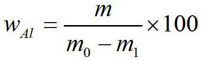
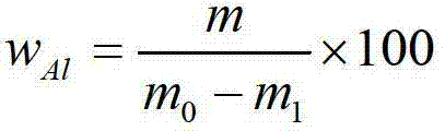
[0044] Take a 15mm×15mm square indium gallium nitride wafer (In0.09Ga0.91N), weighing 532.115mg (m 0 ), the sample is processed by alkali fusion etching, and 0.04g of analytically pure sodium hydroxide is spread on the wafer surface, heated until the sodium hydroxide is completely melted, and after 20 seconds of etching once, the photoluminescence spectrum 340 The substrate peak appeared at nm, and the etching was completed, weighing 531.236mg (m 1 ), then the mass of the etched epitaxial film is 0.879mg (m 0 —m 1 ), with 3mol L -1 Sulfuric acid to adjust the pH of the etching solution to 1, and then use 2mol L -1 Aqueous ammonia to adjust the PH to 3, constant volume.

[0045] (2) Preparation of complexation chromogenic solution

[0046] Take 30ml of etching solution in a 100ml volumetric flask, and add 5.7ml of sulfuric acid (3mol L -1 ), 3ml of potassium iodide solution (1g / ml), 0.5ml of sodium thiosulfate solution (20g / l)...


PUM

PropertyMeasurementUnit
absorbanceaaaaaaaaaa

Abstract

The invention belongs to the technical field of metering test, and relates to a method for testing the indium content in an epitaxial layer of an InGaN chip. The test method comprises the following steps of: carrying out surface etching on the epitaxial layer of the InGaN chip by alkali fusion, neutralizing an etching solution by sulfuric acid, adjusting the acidity of the neutralized etching solution by sulfuric acid or ammonia water, measuring the absorbance of an indium-ethyl violet complexing developing system by a spectrophotometric method, and calculating to obtain the indium content the InGaN chip; and monitoring an etching degree by a deep ultraviolet light photolumineseenee spectrograph, thereby improving the effective transport rate of samples and controlling the etching depth. The standard deviation of repeated measurement is about 1%, and the adding standard recovery is greater than 95%. The test method provided by the invention is suitable for accurately testing the indium content in the epitaxial layer of the InGaN chip, the method can be taken as a validation method for testing the indium content in the epitaxial layer of the InGaN chip by a physical method such as a high resolution X-ray diffraction method and a Rutherford back scattering method, and the method can be also taken as a value fixing method for component standard substance of the epitaxial layer of the InGaN chip.

Description

technical field [0001] The patent of the invention belongs to the technical field of metrology and testing, and relates to the technical field of testing the composition of epitaxial layers of InGaN wafers. Background technique [0002] InGaN (In x Q x N) Semiconductor material is a direct transition wide bandgap material with high luminous efficiency and continuously adjustable bandgap between 0.7eV and 3.4eV. It is widely used in light-emitting devices such as light-emitting diodes (LEDs) and laser diodes (LDs). It can also be used to make ultraviolet detectors and high-temperature and high-power electronic devices. InGaN wafers are usually prepared by metal-organic compound vapor deposition or molecular beam epitaxy. The content of indium in the epitaxial layer of the wafer is closely related to the bandgap width of the material, which is an important indicator for determining the bandgap width of the InGaN material. , accurate determination of the content of indium el...

Claims


Application Information

Patent Timeline
Patent Type & Authority Applications(China)
IPC IPC(8): G01N21/31
Inventor 刘运传王雪蓉孟祥艳周燕萍郑会保魏莉萍
Owner NO 53 RES INST OF CHINA NORTH IND GRP
Why Eureka
Try Eureka