

Textured structure of crystalline silicon solar cell and preparation method thereof
A technology of solar cells and crystalline silicon, applied in the field of solar energy, can solve the problems of low conversion efficiency of solar cells, unfavorable back surface passivation, deep depth, etc., and achieves a simple and easy preparation method, improved conversion efficiency and good compatibility. Effect
- Summary
- Abstract
- Description
- Claims
- Application Information
AI Technical Summary
Problems solved by technology
Method used
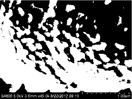
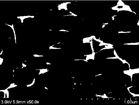
Image

Examples
Embodiment 1
[0052] A method for preparing a textured structure of a polycrystalline silicon solar cell, comprising the steps of:
[0053] (1) Remove and clean the damaged layer of the P-type polysilicon wafer with a thickness of 180±10μm and a size of 156mm×156mm, and then corrode the texture to form a micron-scale texture; then put it into AgNO with a concentration of 0.008mol / L 3 In the solution, react at 20°C for 60 s;
[0054] (2) Put the silicon wafer after the previous step into HF and H 2 o 2 In the mixed solution, the concentrations were 3mol / L and 0.1mol / L respectively, and reacted at 20°C for 300 s;
[0055] (3) Put the silicon wafer after the previous step into a nitric acid solution with a mass percentage of 69% for 300 s, and the cleaning temperature is 20°C;
[0056] (4) Put the silicon wafer after the previous step into a 5% hydrofluoric solution for 200 s by mass, and the cleaning temperature is 20°C;
[0057] (5) Put the silicon wafer after the previous step into 0.05...
Embodiment 2
[0066] A method for preparing a textured structure of a polycrystalline silicon solar cell, comprising the steps of:
[0067] (1) Remove and clean the damaged layer of the P-type polysilicon wafer with a thickness of 180±10μm and a size of 156mm×156mm, and then corrode and make texture to form a micron-scale texture;
[0068] Then put into AgNO with a concentration of 0.008mol / L 3 In the solution, react at 20°C for 60s;
[0069] (2) Put the silicon wafer after the previous step into HF and H 2 o 2 In the mixed solution, the concentrations are 3mol / L and 0.1mol / L respectively, and react at 20°C for 300s;
[0070] (3) Put the silicon wafer after the previous step into a nitric acid solution with a mass percentage of 69% for 300 seconds, and the cleaning temperature is 20°C;
[0071] (4) Put the silicon wafer after the previous step into a 5% hydrogen fluorine solution for 200 seconds, and the cleaning temperature is 20°C;
[0072] (5) Put the silicon wafer after the previou...
Embodiment 3
[0077] A method for preparing a textured structure of a polycrystalline silicon solar cell, comprising the steps of:
[0078] (1) After removing and cleaning the damaged layer of the P-type polysilicon wafer with a thickness of 180±10 μm and a size of 156mm×156mm, etch and make texture to form a micron-scale texture;
[0079] Then put into AgNO with a concentration of 0.008mol / L 3 In the solution, react at 20°C for 60s;
[0080] (2) Put the silicon wafer after the previous step into HF and H 2 o 2 In the mixed solution, the concentrations are 3mol / L and 0.1mol / L respectively, and react at 20°C for 300s;
[0081] (3) Put the silicon wafer after the previous step into a nitric acid solution with a mass percentage of 69% for 300 seconds, and the cleaning temperature is 20°C;
[0082] (4) Put the silicon wafer after the previous step into a 5% hydrogen fluorine solution for 200 seconds, and the cleaning temperature is 20°C;
[0083] (5) Put the silicon wafer after the previou...
PUM
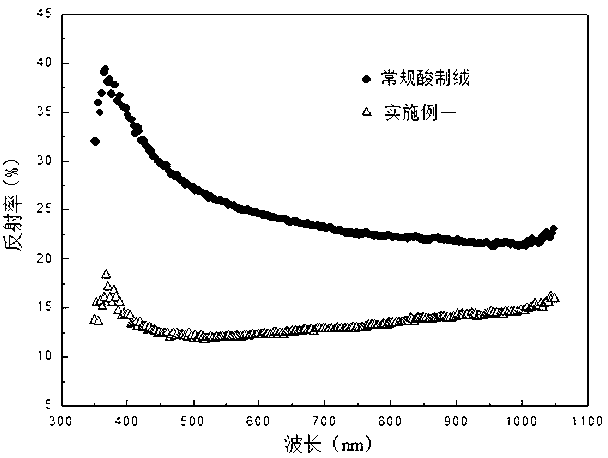
| Property | Measurement | Unit |
|---|---|---|
| reflectance | aaaaa | aaaaa |
| reflectance | aaaaa | aaaaa |
| reflectance | aaaaa | aaaaa |
Abstract
Description
Claims
Application Information