Top-emitting organic light-emitting diode (OLED) device anode structure and preparation technology thereof

An anode structure and device technology, which is applied in the field of preparation of anode structures of top light-emitting OLED devices, can solve problems such as device failure, device disconnection, and yield decline in large-scale production, so as to reduce the hole injection barrier and reduce the probability of short circuit. , the effect of improving stability

Active Publication Date: 2013-07-24
YUNNAN NORTH OLIGHTEK OPTO ELECTRONICS TECH
View PDF8 Cites 12 Cited by
  • Summary
  • Abstract
  • Description
  • Claims
  • Application Information

AI Technical Summary

Problems solved by technology

If the anode and the drive circuit cannot achieve good thermal compatibility and lattice matching, it will cause the device to appear "open circuit", resulting in a large number of device failures, causing a sharp drop in the yield rate of large-scale production

Method used


Image

  • Top-emitting organic light-emitting diode (OLED) device anode structure and preparation technology thereof

Examples


Embodiment 1

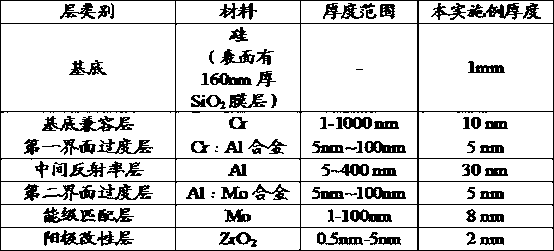
[0026] Embodiment 1: The anode structure of the top-emitting OLED device of the present invention has a base thickness of 1mm, made of silicon and SiO 2 Composition, which is characterized by covering the silicon surface with SiO with a thickness of 160nm 2 film. Four-layer films were prepared on the substrate in the following manner:

[0027] Step 1: Deposit Cr as a substrate-compatible layer on the cleaned substrate to achieve good compatibility with the substrate; the thickness of the substrate-compatible layer is 15 nm, and the thin film adopts PVD such as electron beam evaporation, thermal evaporation, ion beam assisted deposition, and sputtering Method preparation;

[0028] Step 2: Metal Al with low absorption and high reflection characteristics in the visible light band is deposited on the substrate compatible layer as an intermediate reflectivity layer with a thickness of 35 nm. The preparation of the intermediate reflectivity layer meets the requirement of high ref...

Embodiment 2

[0033] Embodiment 2: The anode structure of the top-emitting OLED device of the present invention has a substrate thickness of 1mm, made of silicon and SiO 2 Composition, which is characterized by covering the silicon surface with SiO with a thickness of 160nm 2 film. Cover the substrate with four layers of film in the following manner:

[0034] Step 1: Deposit a substrate-compatible layer made of Cr film on the cleaned substrate to achieve good compatibility with the substrate; the thickness of the substrate-compatible layer is 10nm, and the film is prepared by electron beam evaporation;

[0035] The second step: Deposit the first interfacial transition layer on the substrate compatible layer, which is made of Cr and Al alloys. The film is prepared by the PVD method of a multi-source evaporation system, and the ratio is adjusted by controlling the film growth rate between different components. The film thickness is 5nm;

[0036] Step 3: Depositing metal Al with low absorpt...


PUM


Abstract

The invention relates to the technical field of organic light-emitting diode manufacturing, in particular to preparation of a top-emitting organic light-emitting diode (OLED) device anode structure. The top-emitting OLED device anode structure is characterized in that four layers of thin films cover a substrate, a base compatible layer, a middle reflectivity layer, a energy level matching layer and an anode modifying layer are respectively arranged on the substrate from bottom to top, multifunctionality of an anode is achieved through adoption of the design of a multi-layer thin film structure, light-emitting efficiency of a top-emitting OLED device is obviously improved, and the service life of the top-emitting OLED device is obviously prolonged. Furthermore, due to the fact that the anode is prepared by materials which are not prone to occurrence of element diffusion, probability of occurrence of shot circuit of device pixels due to the element diffusion is reduced. Due to adoption of metallic simple substance or alloy or metallic compound, raw materials can be easily obtained and are low in price, and thin film preparation methods are various.

Description

technical field [0001] The invention relates to the technical field of organic light-emitting diode manufacturing, in particular to the preparation of an anode structure of a top-emitting OLED device. Background technique [0002] OLED is Organic Light-Emitting Diode (Organic Light-Emitting Diode), which has self-illumination, no need for backlight, high contrast, thin thickness, wide viewing angle, and fast response speed. It can be made into solid-state flat panel display panels, solid-state flexible panels and Transparent panel, wide applicable temperature range, simple structure and preparation process and other excellent characteristics. In recent years, through continuous exploration of new materials and further optimization of device structure and process, organic electroluminescent devices have made great progress. However, in order to give full play to their advantages in the flat panel display market, the luminous efficiency of organic electroluminescent devices ,...

Claims


Application Information

Patent Timeline
Patent Type & Authority Applications(China)
IPC IPC(8): H01L51/52H01L51/54H01L51/56
Inventor 王光华段瑜邓荣斌张筱丹季华夏
Owner YUNNAN NORTH OLIGHTEK OPTO ELECTRONICS TECH
Why Eureka
Try Eureka