Preparation and application for silicon quantum dots
A technology of silicon quantum dots and silicon wafers, which is applied in the nanometer field, can solve problems such as high cost of raw materials, silicon quantum dots fall off into the solution, unfavorable chemical modification of biomolecular labeling reactions, etc., and achieve the effect of cheap raw materials and improved efficiency
- Summary
- Abstract
- Description
- Claims
- Application Information
AI Technical Summary
Problems solved by technology
Method used
Image
Examples
Embodiment 1
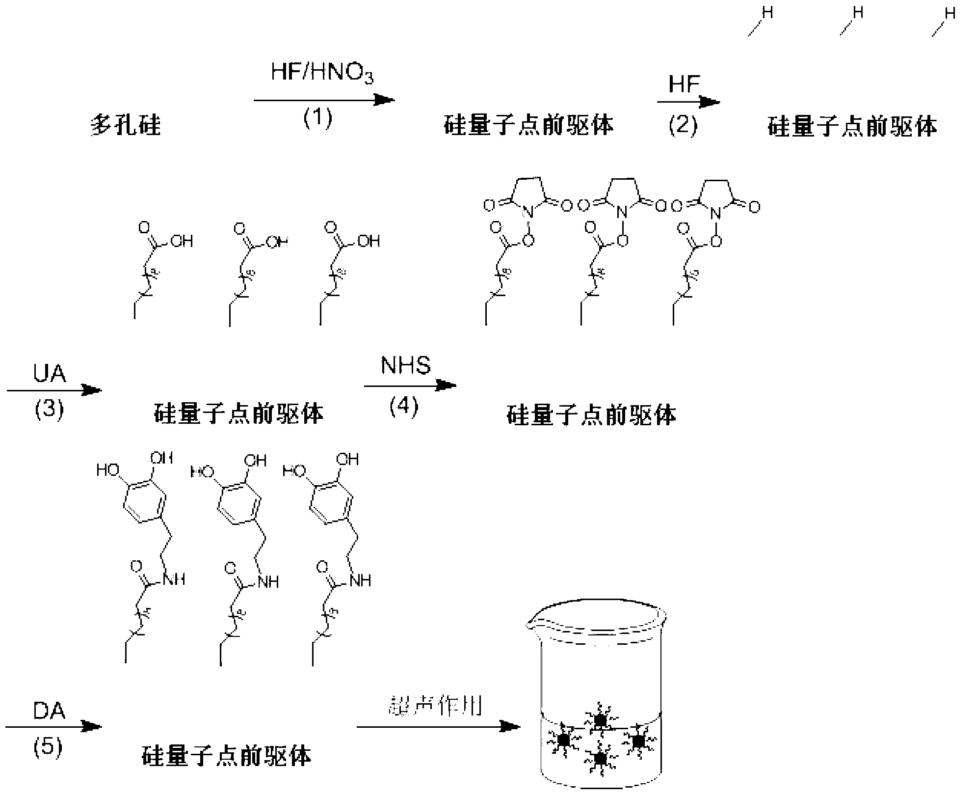
[0039] (1) Clean the planar silicon and immerse it in a mixed aqueous solution of 5.0M hydrofluoric acid and 0.005M silver nitrate for chemical etching reaction. The reaction temperature is controlled at 50°C and the reaction time is 60 minutes;
[0040] (2) Take out the product obtained in step (1), soak it in 33% nitric acid aqueous solution for 20 minutes to remove the remaining Ag, wash it with a large amount of deionized water, and dry it with nitrogen to obtain porous silicon;
[0041] (3) Immerse the porous silicon obtained in step (2) into a mixed aqueous solution composed of 1M hydrofluoric acid and 1M nitric acid to react, control the reaction temperature at 60°C, and the reaction time is 180min to obtain the silicon quantum dot precursor;
[0042] (4) The silicon quantum dot precursor obtained in step (3) was immersed in 5M hydrofluoric acid, the temperature was controlled at 50°C, and the reaction time was 5 minutes to prepare a silicon quantum dot precursor contain...
Embodiment 2
[0048] (1) Same as step (1) of Example 1;
[0049] (2) Same as step (2) of Example 1;
[0050] (3) Immerse the porous silicon obtained in step (2) into a mixed aqueous solution composed of 4M hydrofluoric acid and 1M nitric acid to react, control the reaction temperature at 50°C, and the reaction time is 90min to obtain the silicon quantum dot precursor;
[0051] (4) Same as step (4) of Example 1;
[0052] (5) Same as step (5) of Example 1;
[0053] (6) Same as step (6) of Example 1;
[0054] (7) Same as step (7) of Example 1;
[0055] (8) Same as step (8) of Example 1.
Embodiment 3
[0057] (1) Same as step (1) of Example 1;
[0058] (2) Same as step (2) of Example 1;
[0059] (3) Immerse the porous silicon obtained in step (2) into a mixed aqueous solution composed of 8M hydrofluoric acid and 1M nitric acid to react, control the reaction temperature at 30°C, and the reaction time is 30min to obtain the silicon quantum dot precursor;
[0060] (4) Same as step (4) of Example 1;
[0061] (5) Same as step (5) of Example 1;
[0062] (6) Same as step (6) of Example 1;
[0063] (7) Same as step (7) of Example 1;
[0064] (8) Same as step (8) of Example 1.
[0065] The present invention uses relatively cheap silicon wafers as raw materials, adopts chemical etching method, first prepares porous silicon, and then prepares silicon quantum dot precursors on the silicon wafer substrate, and the etching reaction is carried out at low temperature (not exceeding 60°C) and normal Press down, and after ultrasonic treatment, silicon quantum dots can be obtained. Prope...
PUM
| Property | Measurement | Unit |
|---|---|---|
| particle diameter | aaaaa | aaaaa |
Abstract
Description
Claims
Application Information


