Preparation method of patterned graphene conductive thin film

A graphene film, conductive film technology, applied in carbon-silicon compound conductors, cable/conductor manufacturing, conductive layers on insulating carriers, etc. Short film time, large-scale mass production, and easy availability of raw materials

Inactive Publication Date: 2013-08-07
SHANGHAI NORMAL UNIVERSITY
View PDF7 Cites 34 Cited by
  • Summary
  • Abstract
  • Description
  • Claims
  • Application Information

AI Technical Summary

Problems solved by technology

However, the addition of a surface dispersant will directly affect the conductivity of graphene, resulting in a significant drop in the conductivity

Method used


Image

  • Preparation method of patterned graphene conductive thin film
  • Preparation method of patterned graphene conductive thin film
  • Preparation method of patterned graphene conductive thin film

Examples


Embodiment 1

[0028] The flexible substrate polyimide (PI) was cleaned and dried, and the PI substrate was etched with oxygen plasma. The gas flow rate of etching was 100sccm, the power was 100W, and the etching time was 30s; gravure was used Printing process, the graphene oxide ink with a concentration of 30mg / mL prepared by the Hummers method is evenly brushed on the steel plate with a gravure pattern, and then the ink is embossed on the PI substrate to print a patterned graphene oxide film , and finally put the film in an oven, dry at 80°C for 30 minutes; place the graphene oxide film in a tube furnace filled with inert gas, and anneal at 400°C for 2 hours to obtain a patterned graphene conductive film.

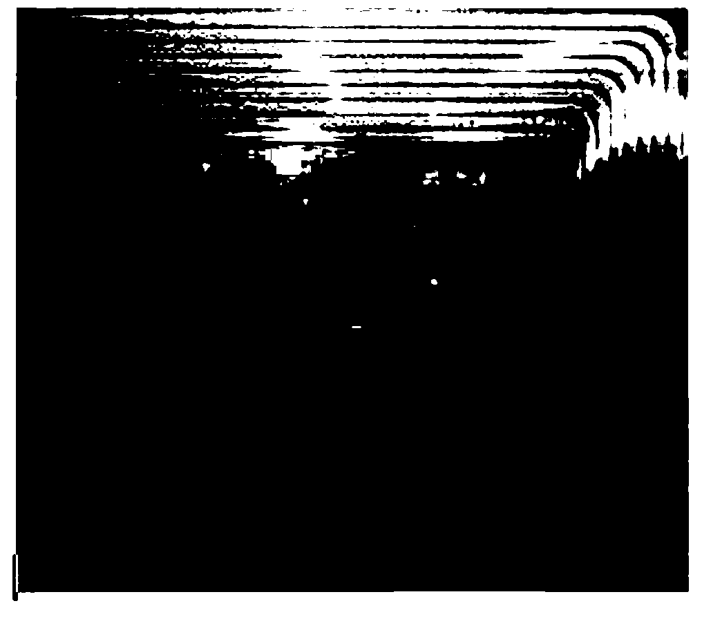
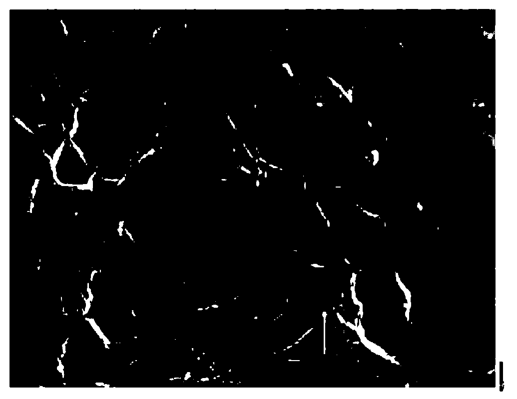
[0029] figure 1 It is an optical microscope image of a patterned graphene conductive film printed on a flexible PI substrate. It can be seen from the figure that the pattern is very clear. figure 2 Field emission scanning electron microscope image of a patterned graphene conductive fi...

Embodiment 2

[0031] The flexible substrate polyimide (PI) was cleaned and dried, and the PI substrate was etched with oxygen plasma. The gas flow rate for etching was 100sccm, the power was 100W, and the etching time was 90s; gravure was used Printing process, the graphene oxide ink with a concentration of 30mg / mL prepared by the Hummers method is evenly brushed on the steel plate with a gravure pattern, and then the ink is embossed on the PI substrate to print a patterned graphene oxide film , and finally put the film in an oven and dry at 80°C for 20 minutes; place the graphene oxide film in a tube furnace filled with inert gas, and anneal at 400°C for 1.5 hours to obtain a patterned graphene conductive film.

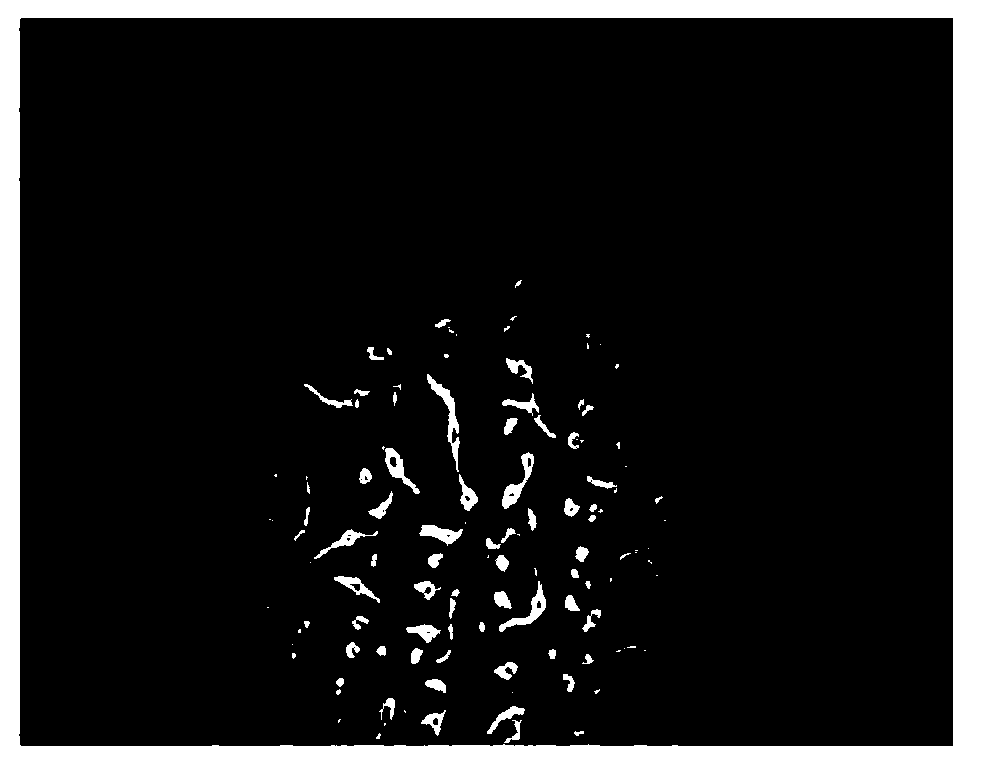
[0032] image 3 It is an optical microscope image of a graphene oxide ink brush with a concentration of 30mg / mL on a PI substrate with an etching treatment time of 90s, and the clarity of the pattern is quite high.

Embodiment 3

[0034] Wash and dry the flexible substrate polyethylene terephthalate (PET), and use oxygen plasma to etch the PI substrate. The gas flow rate for etching is 100 sccm, the power is 100W, and the etching time is 50s; using the gravure printing process, evenly brush the graphene oxide ink with a concentration of 50mg / mL prepared by the Hummers method (after testing, the viscosity of the graphene oxide ink is 62mPa·s) on the steel plate with the gravure pattern , and then imprint the ink on the PET substrate, print a patterned graphene oxide film, and finally put the film in an oven and dry it at 75°C for 30 minutes; put the graphene oxide film in an inert gas In a tube furnace, annealing treatment was performed at 250°C for 2 hours to obtain a patterned graphene conductive film.

[0035] The patterned graphene conductive film prepared in the embodiment was tested for conductivity, and the sheet resistance was 35kΩ / □, which has good conductivity.


PUM

PropertyMeasurementUnit
Viscosityaaaaaaaaaa
Sheet resistanceaaaaaaaaaa

Abstract

The invention belongs to the field of a conductive thin film material and particularly relates to a preparation method of a patterned graphene conductive thin film. The preparation method comprises the following steps of: washing a flexible substrate and drying; utilizing plasmas to treat the flexible substrate; utilizing an intaglio printing process to print graphene oxide printing ink prepared by a Hummers method on the flexible substrate; then putting the flexible substrate into a drying box to be dried to obtain a graphene oxide thin film; and finally, carrying out reduction treatment on the graphene oxide thin film to prepare the patterned graphene conductive thin film. According to the preparation method disclosed by the invention, the patterned graphene conductive thin film is prepared by a manner of combining the graphene oxide printing ink with the intaglio printing process, so that the preparation method is short in film forming time, high in yield and low in production cost; large-scale batch production can be realized; and the prepared patterned graphene conductive thin film is good in flexibility, high in conductivity and high in pattern definition.

Description

technical field [0001] The invention belongs to the field of conductive film materials, in particular to a method for preparing a patterned graphene conductive film. Background technique [0002] Conductive film is a film that can conduct electricity and realize some specific electronic functions, and is widely used in electronic devices such as displays, touch screens and solar cells. At present, indium tin oxide has become one of the main materials for preparing conductive thin films because of its high electrical conductivity and high light transmittance. However, indium tin oxide conductive thin films are brittle and not suitable for the production of next-generation flexible electronic devices, such as bendable LEDs and organic solar cells. Moreover, the raw material price of indium continues to rise, and the cost of the preparation method of indium tin oxide is also very expensive, such as spraying, pulsed laser deposition, electroplating, etc. The unique two-dimensi...

Claims


Application Information

Patent Timeline
IPC IPC(8): H01B5/14H01B1/04B41M1/10H01B13/00
Inventor 黄磊王振平林有杰
Owner SHANGHAI NORMAL UNIVERSITY
Why Eureka
Try Eureka