LED (light emitting diode) epitaxy structure and preparation method thereof

An epitaxial structure and buffer layer technology, applied in semiconductor devices, electrical components, circuits, etc., can solve the problems of low wavelength yield, effectively release lattice mismatch warping, lattice stress, and low crystallinity, and achieve Avoid warpage effect and stress, improve photoelectric performance level, and achieve high wavelength yield

Active Publication Date: 2013-08-07
ANHUI SANAN OPTOELECTRONICS CO LTD
View PDF6 Cites 42 Cited by
  • Summary
  • Abstract
  • Description
  • Claims
  • Application Information

AI Technical Summary

Problems solved by technology

Larger-sized substrates and epitaxial wafers, due to lattice mismatch and thermal expansion coefficient mismatch, will cause greater warpage and lattice stress, and cannot form better secondary wafers that were realized on the original 2-inch small-sized epitaxial wafers. Dimensional layered growth structure, resulting in low crystallinity of the GaN bottom layer, large surface roughness, after the growth of the complete structure, the electrical yield is low, the working voltage VF tends to be too large, and the wavelength is good. The rate is low, and ultimately it is impossible to achieve large-scale mass production of larger-sized epitaxial wafers (such as 4 inches and above)
[0004]Aiming at the above problems, the Chinese invention patent No. 201110451083.2 proposes an insertion layer between the high-temperature non-doped GaN buffer layer and the N-type GaN layer , the insertion layer is an AlxGa1-xN layer or an InyAl1-yN layer Or composed of AlxGa1-xN layers and InyAl1-yN layers stacked, Among them, 0.1F, but cannot release the warpage and lattice stress caused by lattice mismatch and thermal mismatch more effectively at the same time

Method used


Image

  • LED (light emitting diode) epitaxy structure and preparation method thereof
  • LED (light emitting diode) epitaxy structure and preparation method thereof
  • LED (light emitting diode) epitaxy structure and preparation method thereof

Examples


Embodiment 1

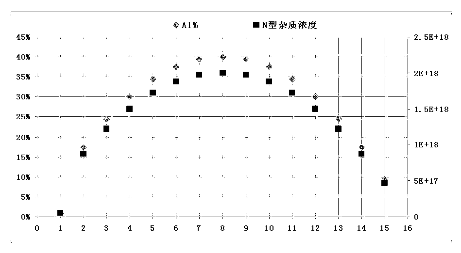
[0027] refer to figure 2 As shown, a kind of AlGaN / n-GaN superlattice bottom layer buffer layer LED epitaxial structure adopting Al composition of the present invention adopts parabolic linear gradient, can be different according to the actual process requirement and application substrate size, present the difference of different number of cycles. Superlattice underlying buffer layer structure with component distribution ratio, the cyclic logarithm ranges from 3 to 40 pairs, and the Al composition in the AlGaN layer ranges from 0% to 40%, and the thickness ranges from 0.1nm to 40nm Take a value between , and the corresponding doping concentration of n-type impurities in the paired n-GaN layer is 5×10 16 cm -3 to 1×10 19 cm -3 The thickness ranges from 0.3nm to 120nm, and the thickness ratio of AlGaN and n-GaN layers is between 1:5 and 1:1; in each AlGaN / n-GaN superlattice buffer layer, The Al composition and n-type doping concentration are uniquely determined by the Al co...

Embodiment 2

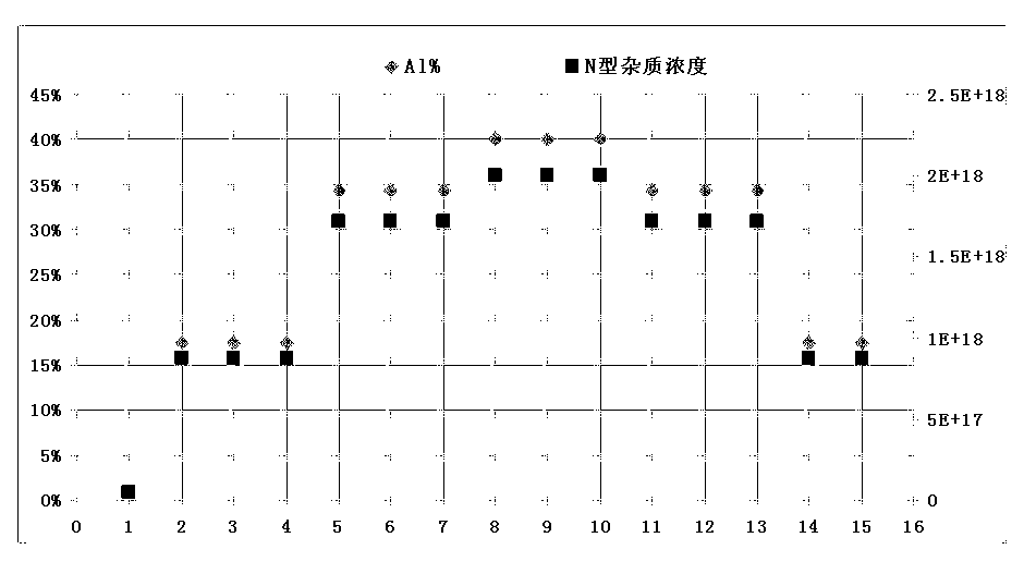
[0033] Different from the optimization scheme of the Al component and n-type impurity concentration ratio coefficient in Example 1 using a parabolic gradual change mode, this embodiment adopts the Al composition and n-type impurity concentration ratio coefficient to gradually increase and then gradually decrease in a stepwise manner. Define that each group of lattice buffer layer pairs is composed of several pairs of AlGaN / n-GaN superlattice buffer layer pairs, Al( m ) represents the m The Al composition value in the AlGaN / n-GaN superlattice buffer layer pair, N ( m ) represents the m The n-type impurity concentration value in the AlGaN / n-GaN superlattice buffer layer pair, Al ( m )and N ( m ) change trend satisfies the relational formula: Al( m ) = Yn *Al( m- 1), N ( m ) = Yn * M ( m- 1), where, Ym follow the parabolic equation , a is a fixed constant, M Represents the total number of groups consisting of several pairs of superlattice buffer layers, m On...


PUM


Abstract

The invention discloses an LED (light emitting diode) epitaxy structure and a preparation method thereof. The LED epitaxy structure successively comprises a substrate, a GaN nucleating layer, multiple pairs of superlattice buffer layers, an n-GaN layer, an MQW luminescent layer, a p-GaN layer and a p-type contact layer from bottom to top, wherein each superlattice buffer layer is formed by an AlGaN/n-GaN alternately stacked structure. The LED epitaxy structure is characterized in that Al(n) is defined to represent an Al component value in the nth pair of AlGaN/n-GaN superlattice buffer layer; N(n) represents the n-type impurity concentration value in the nth pair of AlGaN/n-GaN superlattice buffer layer; the variation trend of Al(n) is gradually lowered after being gradually raised; and the variation trend of N(n) is gradually lowered after being gradually raised. According to the LED epitaxy structure provided by the invention, lattice stress caused by lattice mismatch due to that a sapphire substrate and the GaN lattice are not matched can be effectively and fully released on a bottom layer growth section so as to greatly lower the warping of an epitaxial wafer in the whole high-temperature growth process and improve the wavelength concentricity and yield of the epitaxial wafer. Meanwhile, the GaN lattice quality is effectively improved, the lattice dislocation density is reduced, and the optical-electrical characteristic of the device is more stable.

Description

technical field [0001] The invention relates to an LED light-emitting diode epitaxy (Epitaxy) structure and a preparation method thereof. Background technique [0002] At present, commercial LED epitaxial wafers are mostly made by MOCVD. Due to the lack of a substrate that matches the GaN lattice, GaN-based LED epitaxial wafers are mostly crystallized on substrates of other materials by means of heteroepitaxy. The commonly used heteroepitaxy substrate is sapphire (Al 2 o 3 ), silicon carbide (SiC), etc.; due to the large difference in lattice mismatch and thermal expansion coefficient between GaN and the substrate, it is impossible to directly grow high-quality GaN epitaxial structures. like figure 1 As shown, the existing conventional GaN-based LED epitaxial structure generally adopts a two-step growth method. Taking a sapphire substrate as an example, a layer of underlying GaN nucleation layer is first grown in a low temperature environment (400°C~700°C). Growth at lo...

Claims


Application Information

Patent Timeline
Patent Type & Authority Applications(China)
IPC IPC(8): H01L33/04
CPCH01L33/04H01L33/12H01L33/32H01L33/007H01L33/44H01L33/06H01L33/08H01L2933/0033H01L2933/0025
Inventor 南琦谢祥彬乔楠张文燕周宏敏李兰程伟徐志军吴洪浩
Owner ANHUI SANAN OPTOELECTRONICS CO LTD
Why Eureka
Try Eureka