
Preparation of p-n type nano CuO/alpha-Fe2O3 composite semiconductor material and application thereof as gas sensitive material

A compound semiconductor, -fe2o3 technology, applied in the direction of nanotechnology, nanotechnology, material resistance, etc., can solve the problems of compound semiconductor materials such as hydrogen sulfide and carbon monoxide sensitivity, but there are few researches, so as to achieve good industrial production prospects, high sensitivity, The effect of simple preparation process and equipment

Inactive Publication Date: 2013-08-21
HENAN POLYTECHNIC UNIV
View PDF2 Cites 20 Cited by
  • Summary
  • Abstract
  • Description
  • Claims
  • Application Information

AI Technical Summary

Problems solved by technology

However, for p-n type CuO / α-Fe 2 o 3 The preparation of compound semiconductor materials and their sensitivity to hydrogen sulfide and carbon monoxide are rarely studied

Method used


Image

  • Preparation of p-n type nano CuO/alpha-Fe2O3 composite semiconductor material and application thereof as gas sensitive material
  • Preparation of p-n type nano CuO/alpha-Fe2O3 composite semiconductor material and application thereof as gas sensitive material
  • Preparation of p-n type nano CuO/alpha-Fe2O3 composite semiconductor material and application thereof as gas sensitive material

Examples


Embodiment 1

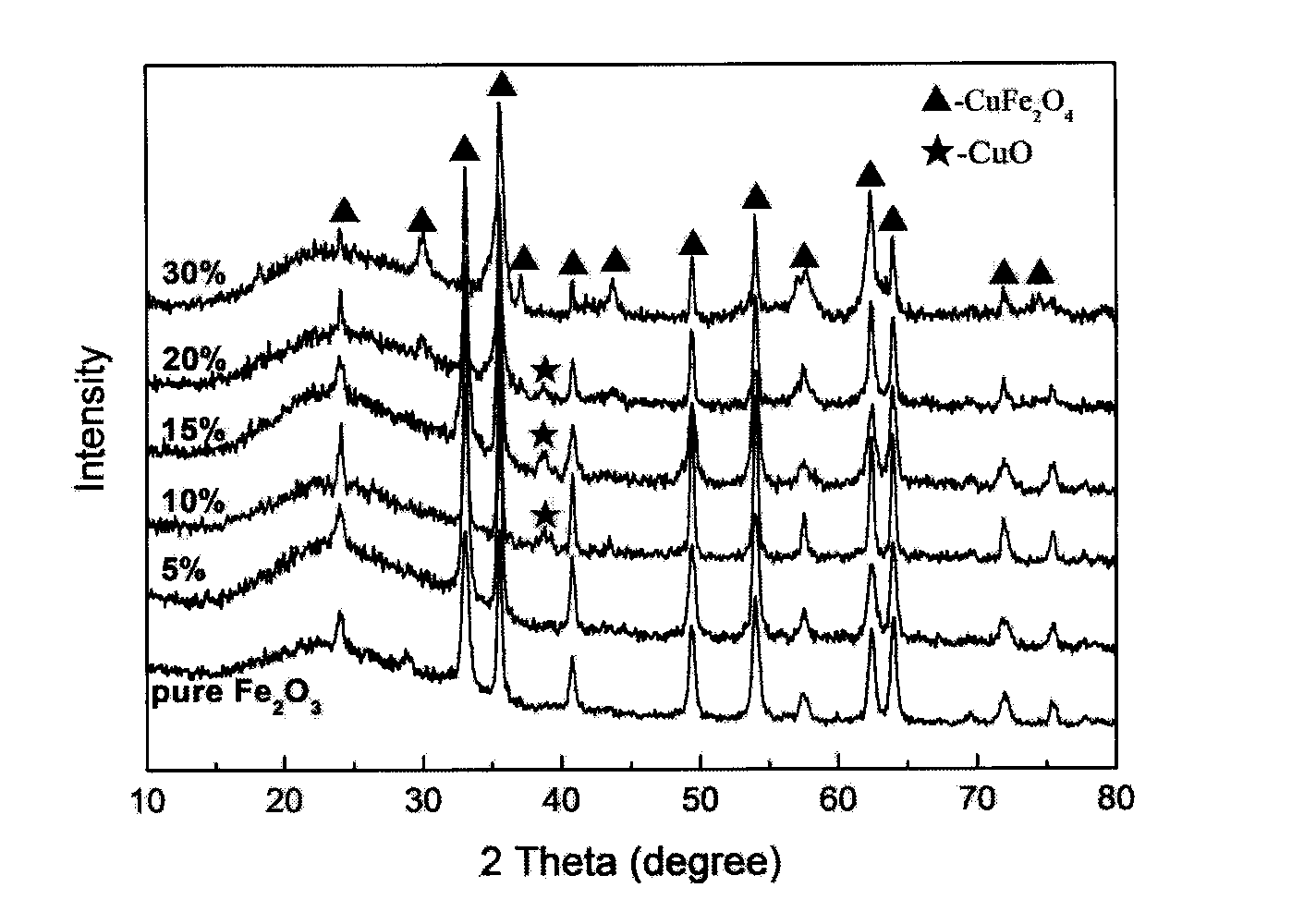
[0022] At room temperature, 0.2M Na 2 CO 3 The solution was added dropwise to 0.2 M Fe(NO 3 ) 3 ·9H 2 O or Cu(NO 3 ) 2 ·3H 2 O aqueous solution, keep the pH value of 8 after the dropwise addition, the obtained precipitate was left to stand for aging for 1 hour, washed several times with deionized water, centrifuged, dried in an oven at 80 °C, and then the product was placed in a muffle furnace in an empty atmosphere. The pure CuO and α-Fe were obtained by calcining at 300 °C for 1 hour. 2 O 3 Nano powder, its XRD analysis is as follows figure 1 shown. A certain amount of prepared α-Fe 2 O 3 The powder was dispersed in Cu(NO) prepared with a CuO mole percentage of 15 mol%. 3 ) 2 ·3H 2 O aqueous solution, the solution was sonicated for 30 min to disperse uniformly. Put 0.2M Na 2 CO 3 The solution was added dropwise to the above aqueous solution under electromagnetic stirring, and the pH value was maintained at 8 after the dropwise addition. The product was left...

Embodiment 2

[0025] The mole percentage of CuO in Example 1 was changed from 15% to 5%, and the others were the same as Example 1. XRD analysis results see figure 1 .

Embodiment 3

[0027] The mole percentage of CuO in Example 1 was changed from 15% to 10%, and the others were the same as Example 1. XRD analysis results see figure 1 .


PUM

PropertyMeasurementUnit
diameteraaaaaaaaaa
particle diameteraaaaaaaaaa

Abstract

The invention relates to a preparation method of a p-n type nano CuO / alpha-Fe2O3 composite semiconductor material, and the material is applied to the field of gas sensors. Pure alpha-Fe2O3 is prepared by using a chemical precipitation method; and the nano CuO / alpha-Fe2O3 composite semiconductor material is further prepared by using a deposition-precipitation method. The CuO / alpha-Fe2O3 composite semiconductor gas sensitive material provided by the invention is simple in preparation technique, low in equipment requirement and low in cost; according to the prepared gas sensitive material, along with the increase of the CuO content, Cu atoms gradually enter alpha-Fe2O3 crystal phases, and the particle sizes of special grains range from 10nm to 20nm. By utilizing the prepared material, effective detection on hydrogen sulfide at room temperature is realized, and the material can rapidly respond to carbon monoxide at both 50 DEG C and 100 DEG C, so that the material has large application prospects.

Description

technical field [0001] The invention relates to a p-n type nanometer CuO / α-Fe 2 O 3 The invention discloses a composite semiconductor material and a preparation method thereof, and is applied to hydrogen sulfide and carbon monoxide gas sensitive materials, belonging to the field of inorganic nanomaterials. Background technique [0002] In order to solve the problem of selectivity of semiconductor resistive gas sensor, Wu Xinghui et al. (Journal of Semiconductors 15(9)(1994)643) proposed the principle of complementary enhancement of gas sensor and the element structure to realize this principle, namely N-N type, P-P type. type, N-P type or P-N type. When the two sensitive bodies of the gas sensor are of different conductivity types (N-P type or P-N type), the new type of component based on this principle is composed of sensitive bodies of two different conductors: N-P type (N-type sensitive body) On the top, the P-type is on the bottom, the output signal voltage is the pot...

Claims


Application Information

Patent Timeline
Patent Type & Authority Applications(China)
IPC IPC(8): G01N27/04B82Y30/00
Inventor 曹建亮王燕孙广李彦伟付乌有孟哈日巴拉张战营
Owner HENAN POLYTECHNIC UNIV
Learn More