Heat insulation structure based on Parylene filling and preparation method thereof

A technology of structural layers and substrates, applied in the field of MEMS, can solve the problems of increasing process complexity, reducing yield, and prone to voids, saving layout area, reducing measurement errors, and improving device performance.

Inactive Publication Date: 2013-09-04
PEKING UNIV
View PDF5 Cites 14 Cited by
  • Summary
  • Abstract
  • Description
  • Claims
  • Application Information

AI Technical Summary

Problems solved by technology

Although this problem can be avoided by etching and filling again, it increases the complexity of the process and reduces the yield
At the same time, long parallel deep grooves are prone to voids during filling. Although it will not affect the thermal insulation performance, it will cause stress concentration and greatly increase the possibility of device failure.
In addition, etching and filling from the front side will affect the active devices on the front

Method used


Image

  • Heat insulation structure based on Parylene filling and preparation method thereof
  • Heat insulation structure based on Parylene filling and preparation method thereof
  • Heat insulation structure based on Parylene filling and preparation method thereof

Examples


Embodiment 1

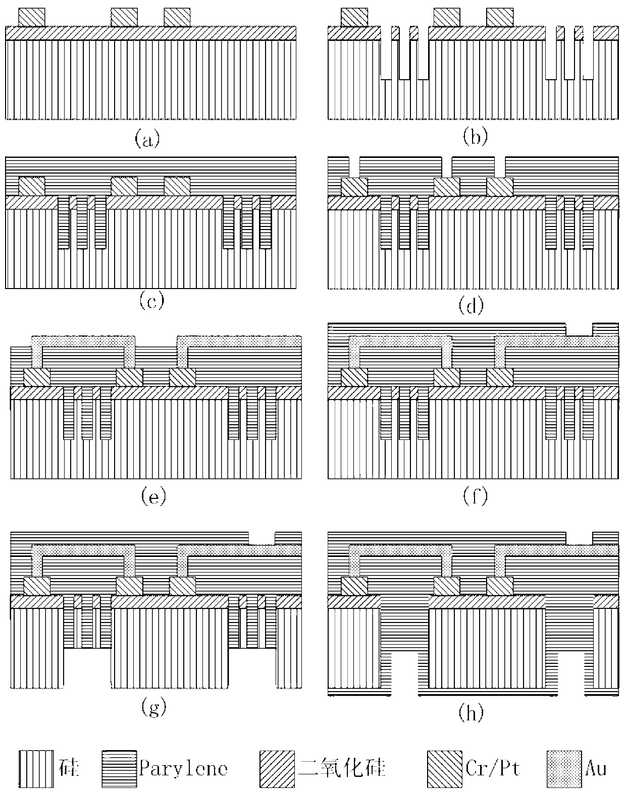
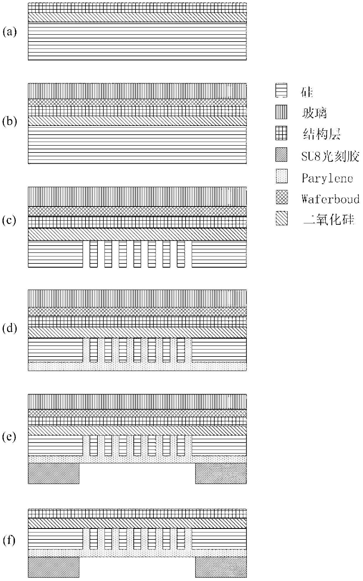
[0030] 1) First, use the usual way to process CMOS circuits or MEMS structures, just ensure that there is a silicon oxide spacer between the base silicon wafer, such as figure 2 (a) shown.

[0031] The spacer acts as an etch stop layer. It can be formed when making the structural layer, or it can be a natural product using the SOI process.

[0032] 2) Use WaferBond temporary bonding agent to bond the glass liner to protect the silicon chip from cracking, such as figure 2 (b) shown.

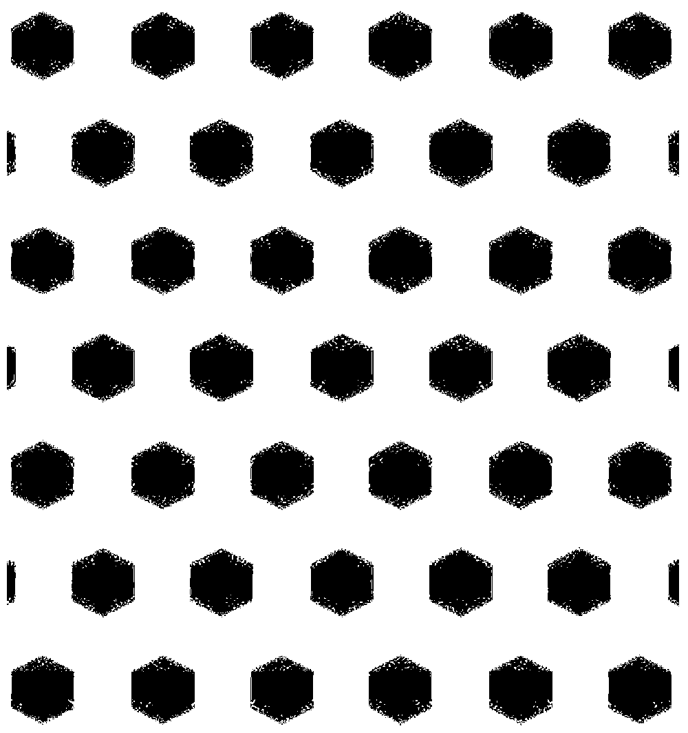
[0033] 3) Thin the silicon wafer from the back to 50um, and perform deep etching in the reserved heat insulation area, leaving substantially equidistant (20um) and uniformly arranged columns, such as figure 2 (c) shown. Columns may be cylinders or prisms with cross-sectional shapes including but not limited to Figure 3a and Figure 3b The quadrilateral and hexagonal structures shown.

[0034] The thickness reduction of the above-mentioned silicon wafer needs to be comprehensively consid...


PUM


Abstract

The invention relates to a heat insulation structure based on a Parylene filling and a preparation method of the heat insulation structure based on the Parylene filling. The preparation method of the heat insulation structure includes the steps of firstly, machining a structural layer on a base silicon wafer, and enabling a silicon oxide interlayer to exist between the structural layer and the base silicon wafer; secondly, adhering a glass lining to the structural layer; thirdly conducting thinning on the back surface of the base silicon wafer, and then conducting deep etching inside a reserved heat insulation region to form evenly arranged column bodies; fourthly, filling Parylene materials in the heat insulation region on the back surface of the base silicon wafer; fifthly, forming a supporting structure on the back surface of the base silicon wafer in a photoetching mode; sixthly, stripping the glass lining which is adhered to the front surface of the base silicon wafer. According to the heat insulation structure based on the Parylene filling and the preparation method of the heat insulation structure based on the Parylene filling, a post CMOS technology can be compatible, effective thermal resistance of the heat insulation region is high, the layout area can be saved in comparison with traditional parallel grooves, limitation for a contour diagram is little, heat insulation performance can be improved, and reliability of a device can be improved.

Description

technical field [0001] The invention belongs to the technical field of MEMS, and in particular relates to a thermal insulation structure based on Parylene filling and a preparation method thereof. Background technique [0002] As a base material commonly used in MEMS technology, silicon has good thermal conductivity. However, for temperature-based sensors such as gas sensors, flow sensors, thermal accelerometers, and infrared sensors, biochemical microreactors such as polymerase chain reaction (PCR) chips, and micro-devices / microsystems such as thermal drives that are highly temperature-dependent , good thermal isolation can significantly reduce power consumption and improve performance. [0003] The basic idea of ​​thermal isolation is to reduce the cross-sectional area of ​​heat transfer or reduce the thermal conductivity of the material. The heat transfer cross-sectional area can be greatly reduced by the insulating film and the air cavity, and a better heat insulation ...

Claims


Application Information

Patent Timeline
IPC IPC(8): B81B7/00B81C1/00
Inventor 陈兢李天宇李男男
Owner PEKING UNIV
Why Eureka
Try Eureka