Coating process of crystalline silicon solar cell

A technology of solar cells and crystalline silicon, which is applied in the coating process of metal materials, circuits, electrical components, etc., and can solve problems affecting the photoelectric conversion efficiency of solar cells, affecting the uniformity of silicon nitride films, uneven temperature and atmosphere, etc. , to achieve the effect of shortening process time, saving ammonia gas and shortening production time

Active Publication Date: 2013-09-11
泗阳腾晖光电有限公司 +1
View PDF4 Cites 6 Cited by
  • Summary
  • Abstract
  • Description
  • Claims
  • Application Information

AI Technical Summary

Problems solved by technology

[0004] At present, the direct PECVD method is used in production to prepare silicon nitride thin films. The production time of each batch is relatively long, including the pre-cleaning step of feeding ammonia gas for a long time (more than 200s) and opening the radio frequency. The main purpose is to use hydrogen ions on the crystal. Silicon surface passivation improves the surface quality of crystalline silicon wafers, but long-term plasma bombardment will cause damage to the surface of crystalline silicon and affect the photoelectric conversion efficiency of solar cells
[0005] In the current coating production process, before plasma sputtering, ammonia gas and silane are injected and waited for 3 to 5 seconds before radio frequency is turned on. The main purpose is to mix the gases evenly, but in a short period of time, the two gases may not be completely mixed evenly. , which will cause inhomogeneity of temperature and atmosphere before coating, and affect the uniformity of silicon nitride film

Method used


Image

  • Coating process of crystalline silicon solar cell
  • Coating process of crystalline silicon solar cell

Examples


Embodiment 1

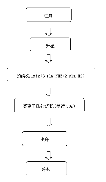
[0038] like figure 1 As shown, a company prepares silicon nitride film by PECVD of polysilicon. Each boat holds 240 silicon wafers. The process is as follows: (1) enter the boat for 2 minutes; (3) Pre-cleaning, the ammonia gas with a flow rate of 3 slm (standard liters / minute) is introduced, and the nitrogen gas with a flow rate of 2 slm (standard liters / minute) is introduced at the same time, and the radio frequency pre-cleaning is turned on for 1 minute; (4) Plasma sputtering For sputtering deposition, the flow rate is 6.8 slm (standard liter / min) ammonia gas and 700 ml / min silane, wait for 30s and start RF plasma sputtering deposition for 13.3 minutes; (5) out of the boat, 2 minutes; (6) cooling, 6 minute.

Embodiment 2

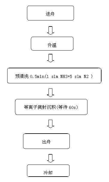
[0040] like figure 2 As shown, embodiment 2 is the coating process of crystalline silicon solar cells of the present invention. A company prepares silicon nitride thin films by single crystal PECVD. Each boat holds 240 silicon wafers. The process is as follows: (1) enter the boat for 2 minutes; ) pre-cleaning, the ammonia gas with a flow rate of 1 slm (standard liter / min) is introduced, and the nitrogen gas with a flow rate of 5 slm (standard liter / min) is introduced at the same time, and the radio frequency pre-cleaning is turned on for 0.5 minutes; (4) Plasma sputtering deposition , the flow rate is 6.8 slm (standard liter / min) ammonia gas and 660 ml / min silane, wait for 60s to open RF plasma sputtering deposition for 13.8 minutes; (5) out of the boat, 2 minutes; (6) cooling, 6 minutes.

[0041] The present invention feeds ammonia and nitrogen at the same time during pre-cleaning, which can not only ensure that hydrogen atoms can passivate defects such as impurities and di...


PUM


Abstract

The invention provides a coating process of a crystalline silicon solar cell. The coating process comprises the following steps of: (1) entering a boat: putting a silicon wafer into a quartz boat; (2) heating after nitrogen is added; (3) precleaning: simultaneously adding nitrogen and ammonia, and turning on radio frequency to preclean; (4) plasma sputtering deposition: adding ammonia and silane, and turning on the radio frequency to perform plasma sputtering deposition; (5) going out of the boat; (6) cooling. The coating process has the beneficial effects that the production time is shortened, the production capacity is improved, and the process running time is shortened by six minutes; the ammonia consumption and the production cost are reduced; the uniformity of a silicon nitride film is improved; the conversion efficiency of the cell is improved; the method is simple and practicable, and additional processing procedures and materials do not need to be added.

Description

technical field [0001] The invention relates to the field of crystalline silicon solar cells, in particular to a coating process for crystalline silicon solar cells. Background technique [0002] The use of plasma vapor deposition (PECVD) to grow silicon nitride films on the surface of crystalline silicon is an important part of the entire production process of crystalline silicon solar cells. It can not only effectively increase the absorption of light by solar cells, but also serve as a passivation layer. It can also effectively passivate the surface of crystalline silicon, which greatly improves the absorption and utilization of light by solar cells. [0003] In the current industrial production, there are two main methods for the preparation of silicon nitride thin films: 1. Direct PECVD method - the silicon wafer is charged as an electrode and directly contacts the plasma; 2. Indirect PECVD method - the silicon wafer is excited without contact Electrodes, deposited on ...

Claims


Application Information

Patent Timeline
Patent Type & Authority Applications(China)
IPC IPC(8): C23C14/34C23C14/00H01L31/18H01L31/0216
CPCY02P70/50
Inventor 胡党平付少剑何伟连维飞苗成祥魏青竹保罗
Owner 泗阳腾晖光电有限公司
Why Eureka
Try Eureka