Double-structure contact hole synchronous-etching technology

A simultaneous etching and contact hole technology, which is applied in the fields of electrical components, semiconductor/solid-state device manufacturing, circuits, etc., can solve the problem of increasing chemical mechanical polishing time of tungsten plugs, increasing process complexity and cost, and unsatisfactory process effects, etc. problem, to avoid the loss of silicon oxide, reduce the abnormal connection, and reduce the effect of process risk

Active Publication Date: 2013-10-02
SHANGHAI HUALI MICROELECTRONICS CORP
View PDF4 Cites 25 Cited by
  • Summary
  • Abstract
  • Description
  • Claims
  • Application Information

AI Technical Summary

Problems solved by technology

Although the above process steps (1)-(6) can use the same photomask to complete the etching of contact holes with different structures in the two regions at the same time, however, in step (7) etching of the bottom silicon oxide barrier layer in the photosensitive area During the process, the logic area will be etched simultaneously, which will bring process defects
[0007] image 3 It is a schematic diagram of the structure in the actual production of the traditional dual-structure contact hole simultaneous etching process; in the actual process production, the thickness of the underlying silicon oxide in the photosensitive area reaches 600A, and in order to remove the silicon oxide of 600A, the etching step must have The total silicon oxide etch removal amount of 900A is used to ensure sufficient process over-etch window, so that the silicon oxide in the STI at the bottom of the borderless contact hole in the logic area and the silicon oxide layer at the top of the contact hole are simultaneously etched eclipse; image 3 As shown, the simultaneous etching of the silicon oxide in the STI at the bottom of the borderless contact hole in the logic area will form a deep hole 19 as deep as 700A-800A on the STI, and the depth of the deep hole 19 is much larger than that of the active layer. The well depth of the ion implantation in the area (AA) (about 500-600A), so that the current in the contact hole will cross the ion-implanted junction and form a path with the substrate silicon after the tungsten plug is filled, causing leakage (leakage), making the device failure; and simultaneous etching of the silicon oxide layer at the top of the contact hole in the logic region will form an excessively large annular chamfer 191 at the top of the contact hole, and this excessive annular chamfer 191 will be formed in the subsequent Ti / TiN When the barrier layer is deposited, it becomes larger due to the bombardment of Ar sputtering (sputter), which can easily cause abnormal communication (contact bridge) between contact holes after tungsten plug deposition and grinding, thus causing device failure
[0008] At present, in order to avoid defects caused by simultaneous etching on silicon oxide in STI at the bottom of the borderless contact hole in the logic area, the general practice is to modify the layout to avoid using borderless contacts hole, and make the size of the contact hole in the logic area (CD) much smaller than the size of the active area (AA) to ensure sufficient pattern alignment (overlay) process window, such as by enlarging the pattern in the active area to avoid Use a borderless contact hole, but it will reduce the integration of the device; or reduce the size of the contact hole to avoid using a borderless contact hole, which will greatly increase the difficulty of the contact hole process
For example, on a 55nm logic chip, the size of the active area (AA) is generally 86nm, and the size of the normal contact hole is 85-90nm, and the contact hole etching process can use the photoresist mask process, but in On a 55nm CIS chip, if the size of AA remains the same, in order to ensure a sufficient process window, the size of the contact hole in the logic area needs to be reduced to about 70nm. This size cannot be achieved by a simple photoresist mask etching process. It requires an amorphous carbon hard mask etching process to complete, and its process complexity and cost are greatly increased
[0009] In addition, in order to avoid defects caused by simultaneous etching of the silicon oxide layer on the top of the contact hole in the logic area, the existing process mainly increases the thickness of the silicon oxide layer as the interlayer dielectric layer (ILD) and increases the filling of the tungsten plug. The final chemical mechanical grinding time is used to cause excessive loss of the ILD silicon oxide layer, thereby reducing the depth of the annular beveled surface at the top of the contact hole, reducing the impact on subsequent processes, and avoiding abnormal communication of the contact hole; however, this method The process is difficult, and the process effect is not very ideal, and it is easy to cause other process problems

Method used


Image

  • Double-structure contact hole synchronous-etching technology
  • Double-structure contact hole synchronous-etching technology
  • Double-structure contact hole synchronous-etching technology

Examples


Embodiment

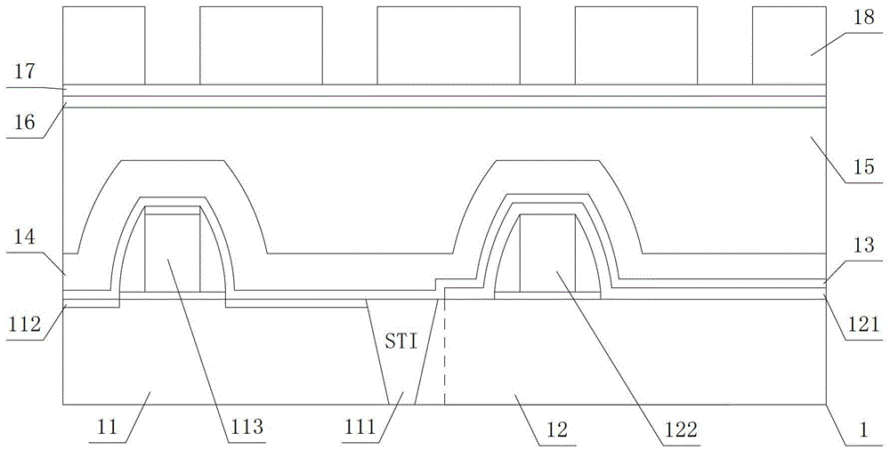
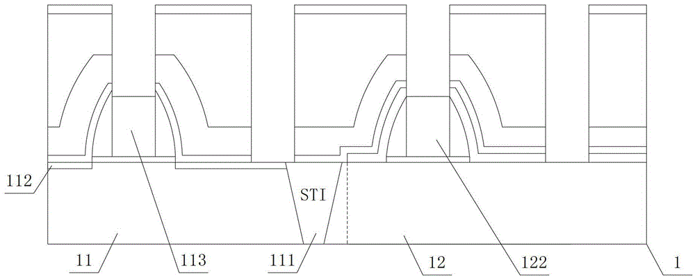
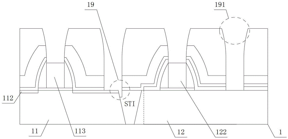
[0044] Figure 4-11 It is a schematic diagram of the flow structure of a dual-structure contact hole simultaneous etching process in the embodiment; as Figure 4-11 As shown, a dual-structure contact hole simultaneous etching process of the present invention:

[0045] First, a substrate 2 with a logic area (logic) 21 and a photosensitive area (pixel) 22 is provided, and the substrate 2 is used to prepare CIS products; the substrate 2 located in the logic area 21 is also provided with shallow trench isolation grooves ( STI) 211, a nickel silicide layer 212 and a first gate structure 213, the nickel silicide layer 212 covers the surface of the substrate 2 not covered by the first gate structure 213 in the logic region and the gate in the first gate structure 213 The upper surface of the electrode; the substrate 2 located in the photosensitive region 22 is provided with a barrier layer (SOR) 221 (preferably, the material of the barrier layer 221 is silicon oxide) and a second ga...


PUM


Abstract

The invention relates to the field of MOS (Metal Oxide Semiconductor) devices, particularly to a double-structure contact hole synchronous-etching technology. The silicon nitride barrier layer in a photosensitive area is removed immediately after a silicon nitride barrier layer is deposited, so that the deposit layer structure of a double-structure contact hole of a CIS (Complementary Metal Oxide Semiconductor Image Sensor) product is changed; the etching selection ratio of an interlayer dielectric layer (insulating dielectric layer) to the barrier layer and a silicone substrate is enlarged in the follow-up etching technology, so that the etching step special for a monox barrier layer at the bottom of the photosensitive area is reduced, the monox loss on STI (Shallow Trench Isolation) of a borderless contact hole in a logic area is reduced while the double-structure contact hole is formed, and the yield of products is improved while the technological reliability and stability are enhanced.

Description

technical field [0001] The invention relates to the field of manufacturing technology of semiconductor MOS devices, in particular to a simultaneous etching process of double-structure contact holes. Background technique [0002] At present, the etching of silicon oxide contact holes is a key process in the etching process. One of the difficulties in the process is that the aperture is small, the etching depth is deep (that is, it has the characteristics of high aspect ratio), and the etching depth varies with the pattern (device) The surface topography changes greatly, especially for CIS (CMOS Image Sensor) products, whose high aspect ratio characteristics are more special. [0003] CIS products have photosensitive area (Pixel) and logic area (Logic) at the same time, which makes its contact hole manufacturing process different from traditional logic or memory chips; Etching process, its specific process flow is as follows: [0004] figure 1 It is a schematic diagram of t...

Claims


Application Information

Patent Timeline
Patent Type & Authority Applications(China)
IPC IPC(8): H01L21/768H01L27/146
Inventor 杨渝书高慧慧吴敏
Owner SHANGHAI HUALI MICROELECTRONICS CORP
Why Eureka
Try Eureka