Hidden-type MEMS pressure sensor sensitive chip and manufacturing method thereof

A technology of pressure sensor and sensitive chip, which is applied in the measurement of the property force of the piezoelectric resistance material, fluid pressure measurement by changing the ohmic resistance, instruments, etc., can solve the problems of device performance and life, and solve the problem of device Reduced performance, improved service life, and reasonable design effects

Inactive Publication Date: 2013-10-09
山西傲维光视光电科技有限公司
View PDF6 Cites 19 Cited by
  • Summary
  • Abstract
  • Description
  • Claims
  • Application Information

AI Technical Summary

Problems solved by technology

[0006] In order to solve the problem of unsatisfactory device performance and service life in the existing silicon piezoresistive pressure sensor, the present invention provides a hidden MEMS pressure sensor sensitive chip and its manufacturing method

Method used


Image

  • Hidden-type MEMS pressure sensor sensitive chip and manufacturing method thereof
  • Hidden-type MEMS pressure sensor sensitive chip and manufacturing method thereof
  • Hidden-type MEMS pressure sensor sensitive chip and manufacturing method thereof

Examples


Embodiment 1

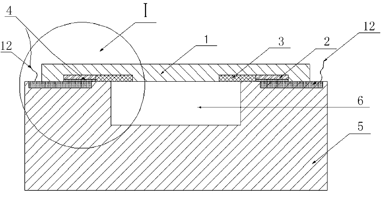
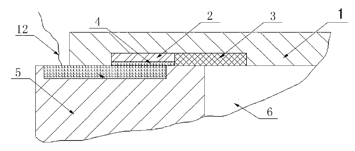
[0039] like figure 1 , 2 As shown, a sensitive chip of a hidden MEMS pressure sensor includes an SOI sheet device layer 1 (that is, as a sensitive film of a pressure sensor, and the SOI sheet is etched by a wet or dry etching process with the BOX layer of the SOI sheet as a stop layer. Formed after the substrate layer) and glass substrate 5.

[0040] Four piezoresistors R1, R2, R3, R4 of the Wheatstone bridge, eight doped wires 3 and eight connection anchor points 2 for connection are made on the SOI sheet device layer 1, and the Both ends of each varistor are connected to one end of a respective doped wire 3, and the other end of each doped wire 3 is overlapped with a respective connection anchor point 2; each connection anchor point 2 A layer of metal layer 4 forming an ohmic contact is formed on it.

[0041] The upper surface of the glass substrate 5 is corroded with a pressure chamber 6 with a depth of 5-200 μm and the first, second, third, fourth and fifth mosaic circu...

Embodiment 2

[0044] The manufacturing method of the hidden MEMS pressure sensor sensitive chip described in the above-mentioned embodiment 1 comprises the following steps:

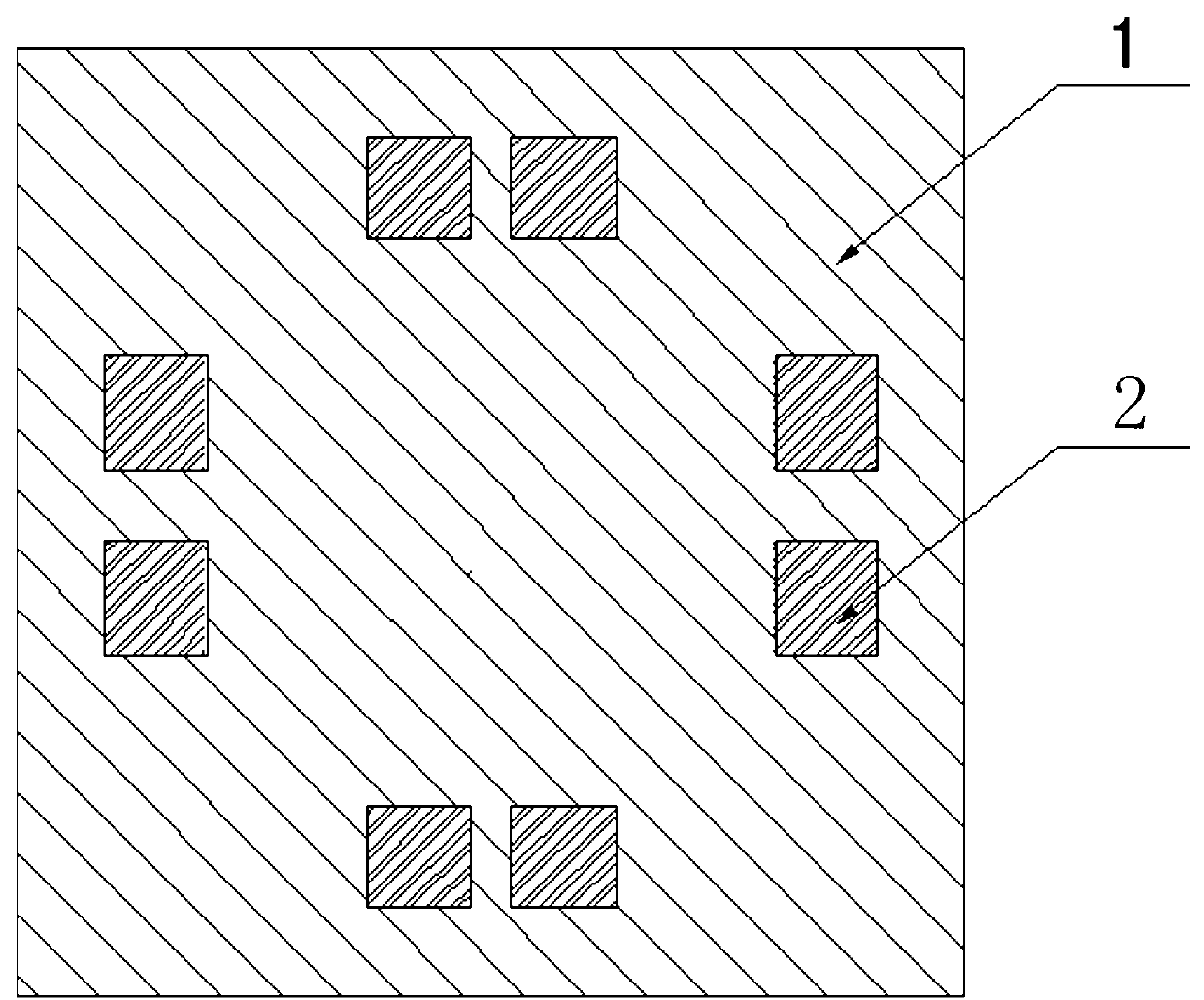
[0045] (1) Perform high-concentration diffusion, ion implantation process or growth of highly doped polysilicon on the SOI device layer 1 to form eight highly doped connection anchor points 2; as image 3 shown. For example, for P-type high doping, the concentration is required to be 10 19 cm -3 above.

[0046] (2) Perform ion implantation on the device layer 1 of the SOI sheet, and inject ion dose Φ=(4~8)×10 14 / cm 2 , the injection energy is 80~200KeV, making four piezoresistors R1, R2, R3, R4 of the Wheatstone bridge and eight doped wires 3 for connection; the two ends of each piezoresistor are all connected to one end of the respective doped wire 3, and the other end of each doped wire 3 is overlapped with the respective connection anchor point 2; as Figure 4 shown.

[0047] (3) Sputtering the metal layer 4...


PUM


Abstract

The invention relates to a sensitive chip of a pressure sensor, in particular to a hidden-type MEMS pressure sensor sensitive chip and a manufacturing method thereof. According to the hidden-type MEMS pressure sensor sensitive chip and the manufacturing method, the problem that component performance and service life of an existing silicon piezoresistive pressure sensor are not ideal is solved. The hidden-type MEMS pressure sensor sensitive chip comprises an SOI wafer component layer (1) and a glass substrate (5), wherein the SOI wafer component layer (1) is formed by the practice that a substrate layer of an SOI wafer is etched in an etching process based on a stopping layer, and the BOX layer of the SOI wafer is taken as the stopping layer. Four voltage dependent resistors of the Wheatstone bridge including R1, R2, R3 and R4, eight doping wires (3) and eight connection anchor points (2) are manufactured on the SOI wafer component layer (1). The hidden-type MEMS pressure sensor sensitive chip and the manufacturing method are reasonable in design, the manufacture hidden-type MEMS pressure sensor sensitive chip overcomes influences of external environment factors on a component circuit, the defect that component performance is reduced due to thermal mismatch of materials is eliminated, and service life of components is prolonged.

Description

technical field [0001] The invention relates to a sensitive chip of a pressure sensor and a manufacturing method thereof, in particular to a sensitive chip of a hidden MEMS pressure sensor and a manufacturing method thereof. Background technique [0002] At present, pressure sensors are widely used in defense industry, automobile industry, petroleum industry, aerospace, medical equipment and consumer electronics and other fields. [0003] In various application fields of sensors, temperature, flow, pressure, and position are the most common test parameters. Among all kinds of sensors, because the pressure sensor can be widely used in the measurement and control of pressure, height, liquid flow, flow velocity, liquid level, and pressure, it has become a type of sensor with the most mature sensor technology and stable performance ratio. According to the Japan Electric Measuring Instrument Industry Association's statistics on the production and sales of process sensors (temper...

Claims


Application Information

Patent Timeline
Patent Type & Authority Applications(China)
IPC IPC(8): G01L9/06G01L1/18B81B7/00B81C1/00
Inventor 陈旭远郑小杉伞海生
Owner 山西傲维光视光电科技有限公司
Why Eureka
Try Eureka