Preparation method for germanium substrate and La-based high-dielectric constant gate dielectric material

A high dielectric constant, gate dielectric technology, used in circuits, electrical components, semiconductor/solid-state device manufacturing, etc. The effect of desorption and volatilization, improvement of anti-radiation performance, and improvement of surface roughness

Active Publication Date: 2013-10-23
XIDIAN UNIV
View PDF6 Cites 5 Cited by
  • Summary
  • Abstract
  • Description
  • Claims
  • Application Information

AI Technical Summary

Problems solved by technology

But Ge oxide GeO 2 The thermal stability of germanium oxide is poor, and it will be thermally decomposed above 500°C. At the same time, its dielectric constant is low. In order to improve the thermal stability of germanium oxide and obtain a smaller equivalent oxide layer thickness, it needs Bottom growth of high dielectric constant materials for better electrical properties
[0005] On the other hand, during the high-temperature annealing process of the Ge substrate, GeO will be adsorbed and volatilized on the surface, which will deteriorate the roughness of the surface of the high dielectric constant gate dielectric.
Moreover, the gate dielectric without heat treatment will have defects, which will increase the probability of leakage current when the gate dielectric is integrated into the semiconductor device, and the loose amorphous structure of the high dielectric constant gate dielectric is not conducive to the improvement of its performance.
[0006] As a traditional metal oxide deposition process, metal organic compound chemical vapor deposition MOCVD, molecular beam epitaxy growth MBE and other processes grow gate dielectric materials with poor step coverage and large surface roughness leading to poor film interface quality , which will seriously affect the overall quality of the film, thereby affecting the reliability of the device, and its higher growth temperature does not conform to the trend of the semiconductor industry towards lower thermal budgets

Method used


Image

  • Preparation method for germanium substrate and La-based high-dielectric constant gate dielectric material
  • Preparation method for germanium substrate and La-based high-dielectric constant gate dielectric material
  • Preparation method for germanium substrate and La-based high-dielectric constant gate dielectric material

Examples


example 1

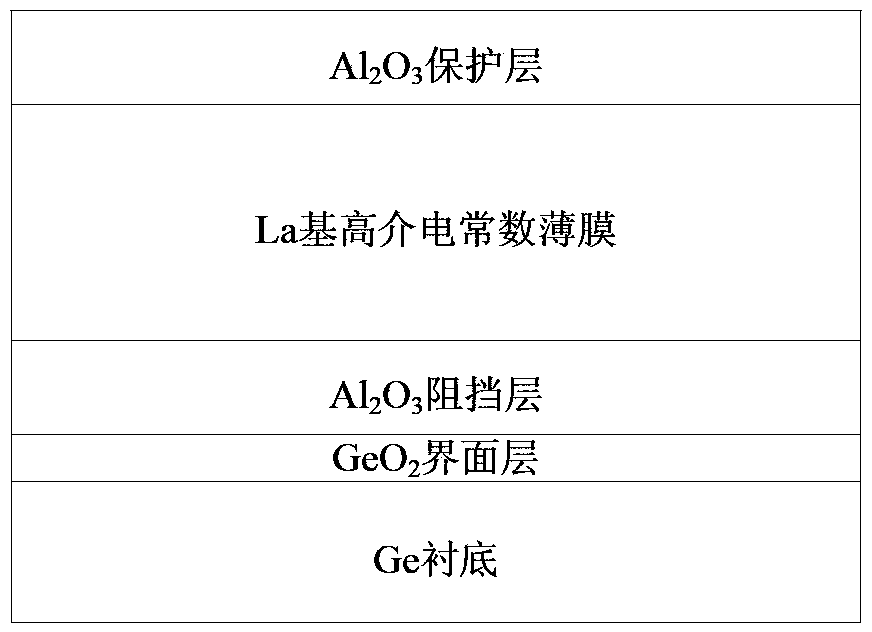
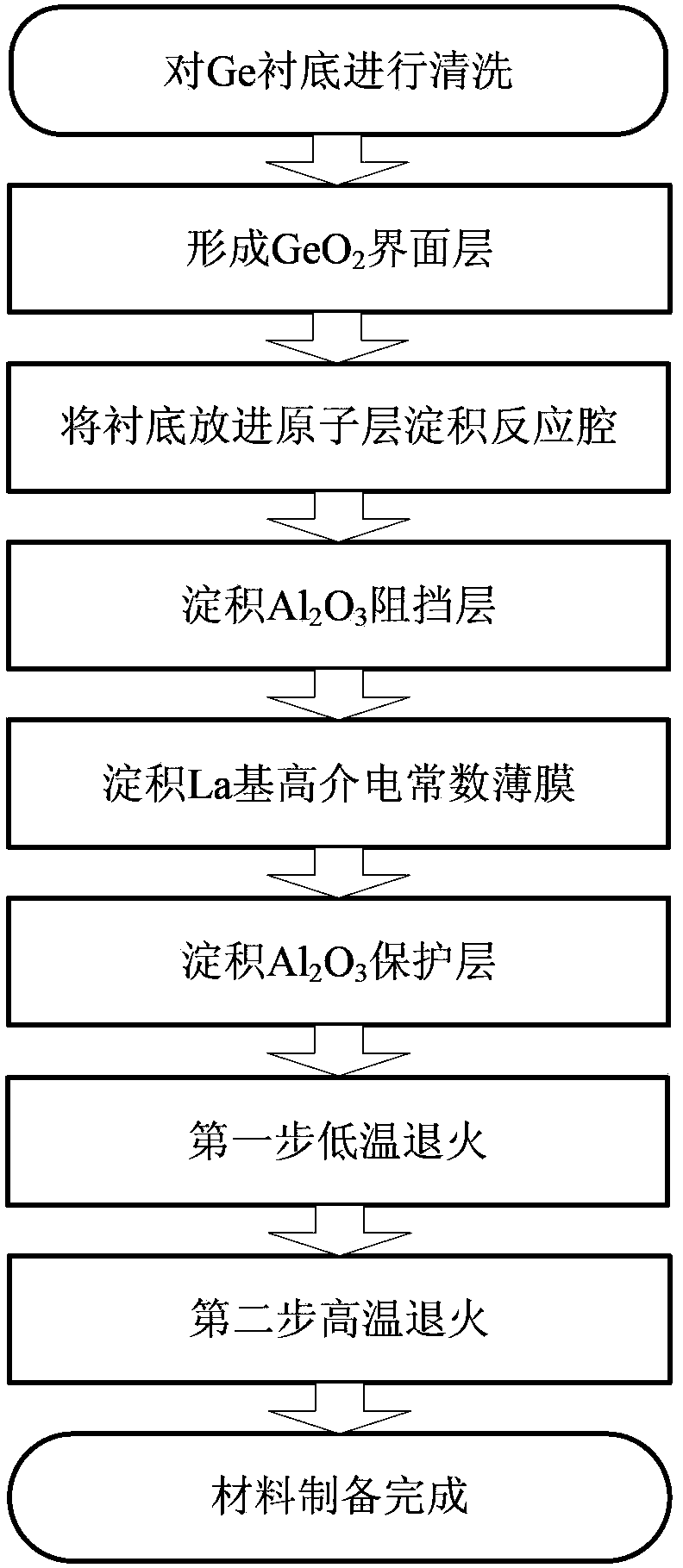
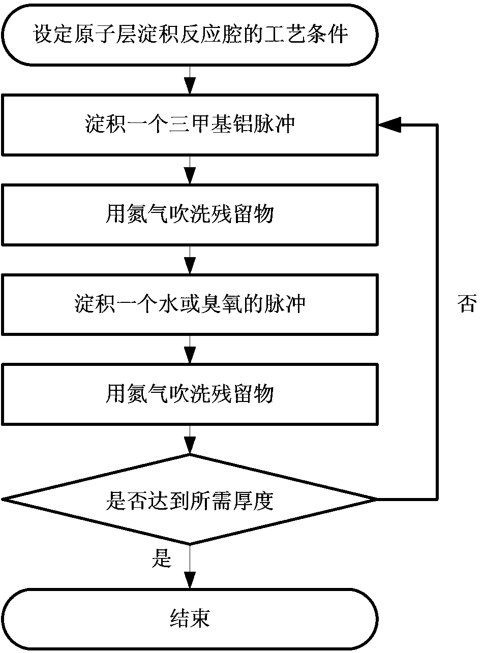
[0056] Example 1, preparation of Al 2 O 3 \La 2 O 3 \Al 2 O 3 \GeO 2 \Ge high dielectric constant gate dielectric material

[0057] Step 1, cleaning the Ge substrate.

[0058] 1a) Clean the Ge substrate in an SC-1 solution heated to 75°C for 10 minutes. The composition of the solution is NH 4 OH, H 2 O 2 and H 2 O, its ratio is 5:1:1, the main effect of this cleaning is to rely on NH 4 Complexation of OH with H 2 O 2 Strong oxidizing ability to remove organic pollutants or attached particles on Ge wafers;

[0059] 1b) Rinse the Ge sheet after cleaning in the SC-1 solution in deionized water for 2 minutes to remove the residual SC-1 solution;

[0060] 1c) Wash the Ge chip in HF solution for 60 seconds, the composition of the solution is HF and H 2 O, whose ratio is 1:400, the main function of this cleaning is to remove the natural oxide layer GeO on the surface of the Ge substrate. 2 ;

[0061] 1d) rinsing the Ge sheet from which the natural oxide layer on the ...

example 2

[0091] Example 2, preparation of Al 2 O 3 \LaAlO 3 \Al 2 O 3 \GeO 2 \Ge high dielectric constant gate dielectric material

[0092] Step 1, cleaning the Ge substrate.

[0093] 1.1) Clean the Ge chip in the SC-1 solution heated to 75°C for 10 minutes. The composition of the solution is NH 4 OH, H 2 O 2 and H 2 O, its ratio is 5:1:1, the main effect of this cleaning is to rely on NH 4 Complexation of OH with H 2 O 2 Strong oxidizing ability to remove organic pollutants or attached particles on Ge wafers;

[0094] 1.2) Rinse the Ge sheet after cleaning in the SC-1 solution in deionized water for 2 minutes to remove the residual SC-1 solution;

[0095] 1.3) Wash the Ge chip in HF solution for 60 seconds, the composition of the solution is HF and H 2 O, whose ratio is 1:400, the main function of this cleaning is to remove the natural oxide layer GeO on the surface of the Ge substrate. 2 ;

[0096] 1.4) Rinse the Ge sheet in deionized water to remove residual HF solut...

example 3

[0128] Example 3, preparation of Al 2 O 3 \HfLaO\Al 2 O 3 \GeO 2 \Ge high dielectric constant gate dielectric material

[0129] Step A, cleaning the Ge substrate.

[0130] Clean the Ge sheet in an SC-1 solution heated to a temperature of 75°C for 10 minutes to remove organic pollutants or attached particles on the Ge sheet. The composition of the solution is NH 4 OH, H 2 O 2 and H 2 O, the ratio is 5:1:1; then rinse the Ge sheet in deionized water for 2 minutes in SC-1 solution to remove residual SC-1 solution; then wash the Ge sheet in HF and H 2 O ratio is 1:400 in the HF solution cleaning 60 seconds, to remove the natural oxide layer of Ge substrate surface; The Ge plate that removes the natural oxide layer of Ge substrate surface is rinsed in deionized water again, to remove residual HF Solution; put the Ge sheet that removes the residual HF solution into deionized water and use ultrasonic cleaning for 5 minutes to remove the adsorption particles on the surface, a...


PUM

PropertyMeasurementUnit
thicknessaaaaaaaaaa
thicknessaaaaaaaaaa
thicknessaaaaaaaaaa

Abstract

The invention discloses a preparation method for a germanium substrate and La-based high-dielectric constant gate dielectric material. The problems of low dielectric constant and poor thermal stability and thin film compactness of the conventional material are mainly solved. The gate dielectric material comprises an interface layer (1), a barrier layer (2), an La-based high-dielectric constant thin film (3) and a protective layer (4) from bottom to top, wherein the interface layer (1) is made from 0.5 to 1nm thick GeO2; the barrier layer (2) is made from 0.5 to 2nm thick Al2O3; the La-based high-dielectric constant thin film (3) is made from 1 to 10nm thick La2O3 or LaAlO3 or HfLaOx; and the protective layer (4) is made from 1 to 2nm thick Al2O3. The whole material is prepared by an atomic layer deposition method, and is subjected to low-temperature and high-temperature annealing treatment after being prepared. The germanium substrate and La-based high-dielectric constant gate dielectric material has the advantages of high dielectric constant, high thin film compactness, high step coverage, high thermal stability and low surface roughness, and can be used for manufacturing a gate dielectric film of a metal oxide semiconductor field effect transistor.

Description

technical field [0001] The invention belongs to the technical field of semiconductor materials, and in particular relates to a preparation method of a La-based high-permittivity gate dielectric material based on a germanium substrate, which can be used to manufacture gate dielectric films of metal oxide semiconductor field effect transistors. Background technique [0002] With the continuous reduction of the integration level of integrated circuits, the size of the metal oxide semiconductor field effect transistor MOSFET is continuously reduced, and the corresponding gate oxide thickness is also continuously reduced. Leakage caused by electron tunneling is increasing exponentially, and the resulting high power consumption and reliability problems are becoming more and more severe. In order to reduce the power consumption increase caused by gate oxide leakage, Intel successfully introduced high dielectric constant gate dielectric materials in the 45nm CMOS process. Due to th...

Claims


Application Information

Patent Timeline
Patent Type & Authority Applications(China)
IPC IPC(8): H01L29/51H01L21/28H01L21/285
Inventor 刘红侠范小娇费晨曦卓青青汪星尹淑颖
Owner XIDIAN UNIV
Why Eureka
Try Eureka