Polarization doping-based GaN Schottky diode
A Schottky diode, polarization doping technology, applied in electrical components, circuits, semiconductor devices, etc., can solve the problem of not carrying out the preparation of polarization doped GaN Schottky diode devices, etc., to improve the Q value, Improve the operating frequency and output power, reduce the effect of series resistance
- Summary
- Abstract
- Description
- Claims
- Application Information
AI Technical Summary
Problems solved by technology
Method used
Image

Examples
Embodiment 1
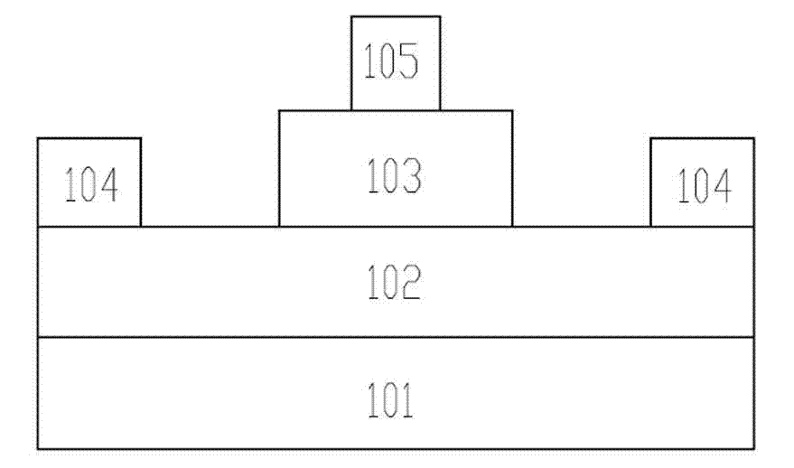
[0020] Depend on figure 1 As shown, it can be seen that the GaN Schottky diode based on polarization doping includes a semi-insulating substrate layer 101 for supporting the entire GaN Schottky diode, and a highly doped N+ type GaN grown on the substrate layer 101. layer 102 and the N-type Al grown on the N+-type GaN layer 102 using polarization doping x Ga 1-x N (0x Ga 1-x The Al composition of the N (016 cm -3 to 10 19 cm -3 .
[0021] An ohmic contact electrode 104 is grown on the N+ type GaN layer 102, the ohmic contact electrode 104 is divided into two parts, symmetrically arranged at both ends of the N+ type GaN layer 102, between the ohmic contact electrode 104 and the N+ type GaN layer 102 surface contact. In the N-type Al x Ga 1-x A Schottky contact electrode 105 is grown on the N (0x Ga 1-x The N (0<x≦1) layers 103 are in contact with each other.
[0022] In this embodiment, the substrate layer 101 is a sapphire substrate; the ohmic contact electrode 104 i...
Embodiment 2
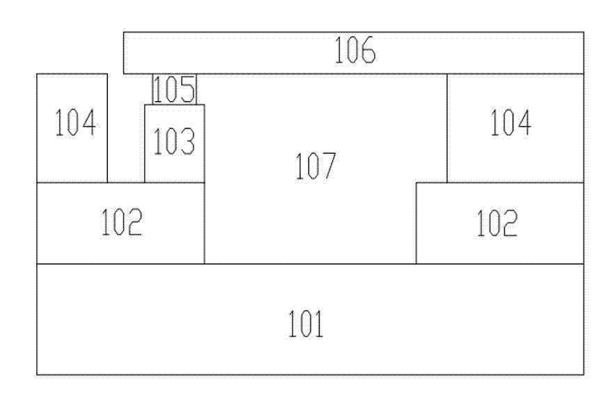
[0031] Depend on figure 2 It can be seen that, unlike Example 1, the N-type Al x Ga 1-x The Al composition of the N (0
[0032] The N+-type GaN layer 102 is divided into two parts and arranged at both ends of the substrate layer 101, on which ohmic contact electrodes 104 are respectively arranged, and one of the N+-type GaN layers 102 is also provided with an N-type Al x Ga 1-x N (0x Ga 1-x A Schottky contact electrode 105 is arranged on the N (0<x≤1) layer 103, and an air bridge cantilever 106 is arranged on the upper surface of the Schottky contact electrode 105 and the ohmic contact electrode 104 on the other side. Below the cantilever 106 is a deep trench isolation region 107 .
[0033] Below the air bridge cantilever 106, there is a deep groove isolation region 107, which connects the Schottky contact electrode 105, the ohmic contact electrode 104 connected to the air bridge cantilever 106, and...
Embodiment 3
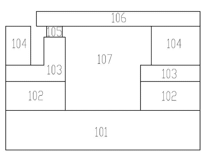
[0046] Such as image 3 It can be seen that, different from Embodiment 2, the N+ type GaN layer 102 is divided into two parts and arranged at both ends of the substrate layer 101, and the N+ type GaN layer 102 is provided with an N-type Al x Ga 1-x N (0x Ga 1-x The N (0x Ga 1-x There are steps on the N (0
[0047] There are also differences in the manufacturing process. Corresponding to step 4 in embodiment 2, step 4 of this embodiment should be: remove N-type Al by wet etching or dry etching process x Ga 1-x Part of the N (0x Ga 1-x At the bottom of the N (0x Ga 1-x Steps are formed on the N (0x Ga 1-x On the bottom of the N (0<x≤1) layer 103, the ohmic contact electrode 104 is formed ...
PUM
 Abstract
Description
Claims
Application Information
PatSnap Eureka turns technology decisions into work you can execute. Powered by our Innovation Knowledge Graph, it runs expert workflows across engineering, life sciences, materials and intellectual property. Get your review-ready output in minutes.


