

Preparation method of high-orientation conductive polymer film, prepared film and application thereof
A conductive polymer and high-orientation technology, which is applied in the manufacture of semiconductor/solid-state devices, circuits, electrical components, etc., can solve problems such as poor solubility, difficulty in preparing oriented films, complicated procedures, etc., and achieve the effect of high degree of orientation
- Summary
- Abstract
- Description
- Claims
- Application Information
AI Technical Summary
Problems solved by technology
Method used
Image

Examples
preparation example Construction
[0029] The preparation method of the highly oriented conductive polymer film of the present invention is specifically:
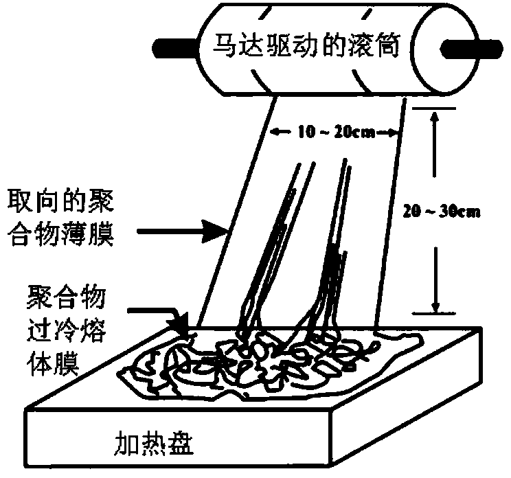
[0030] The preparation method of highly oriented polymer film is as figure 2 As shown, it is a melt stretching method, and the specific steps are as follows: pour an appropriate amount of polymer solution on a preheated smooth glass plate (with a heating plate under it) and spread it evenly. After the solvent is completely evaporated, a mechanical roller (such as a motor-driven roller) is used to stick and stretch the polymer supercooled melt film on the glass plate to obtain a highly oriented polymer film. Both the thickness and the degree of orientation of the film depend on the concentration of polymer, the preheating temperature of the glass sheet and the stretching rate of the mechanical rollers. The thickness of the highly oriented polymer film produced by the present invention is preferably between 30-100nm, and the size is: width 5-30cm, length 5-3...
Embodiment 1
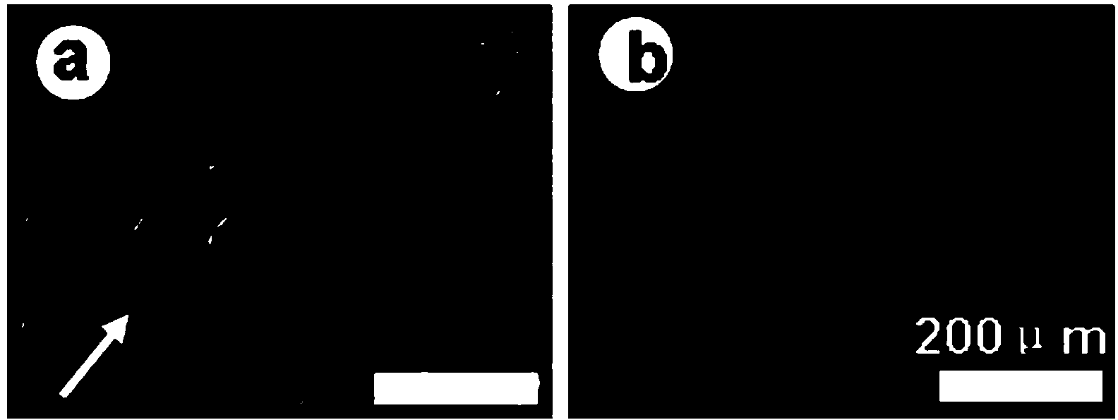
[0040] The electrode of electrochemical polymerization uses ITO modified by melt-stretched oriented PVDF film as the working electrode, Ti sheet as the counter electrode, Ag / Ag + The anhydrous electrode is the reference electrode, the solvent is acetonitrile / dichloromethane (1 / 1), and the composition of the electrolyte solution is: 3-methylthiophene (1mg.ml -1 ), phosphorus hexafluoride tetra-n-butylamine (0.1mol.l -1 ). The polymerization process adopts the mode of cyclic voltammetry, the scanning voltage is: -0.2-1.2V, the scanning speed is 40mV / S, and the number of cycles is 50 times. The prepared highly oriented conductive polymer film has a thickness of 700nm and an anisotropy ratio of conductivity of 59.
Embodiment 2
[0042] The electrode of electrochemical polymerization uses ITO modified by melt-stretched oriented PP film as the working electrode, Ti sheet as the counter electrode, Ag / Ag + The anhydrous electrode is the reference electrode, the solvent is acetonitrile / dichloromethane (1 / 1), and the composition of the electrolyte solution is: 3-methylthiophene (1mg.ml -1 ), phosphorus hexafluoride tetra-n-butylamine (0.1mol.l -1 ). The polymerization process adopts the mode of cyclic voltammetry, the scanning voltage is: -0.2-1.2V, the scanning speed is 40mV / S, and the number of cycles is 50 times. The prepared highly oriented conductive polymer film has a thickness of 700nm and an anisotropy ratio of conductivity of 50.
PUM
| Property | Measurement | Unit |
|---|---|---|
| thickness | aaaaa | aaaaa |
| thickness | aaaaa | aaaaa |
| thickness | aaaaa | aaaaa |
Abstract
Description
Claims
Application Information