Epitaxial growth method and structure of light-emitting diode (LED) structure including potential barrier with gradually-varied thickness

A technology of LED structure and epitaxial growth, applied in electrical components, circuits, semiconductor devices, etc., can solve the problems affecting LED light efficiency, uneven distribution of electrons and holes, etc., to improve LED light efficiency, reduce resistance, improve The effect of resistance

Active Publication Date: 2013-12-25
XIANGNENG HUALEI OPTOELECTRONICS
View PDF7 Cites 3 Cited by
  • Summary
  • Abstract
  • Description
  • Claims
  • Application Information

AI Technical Summary

Problems solved by technology

[0006] The purpose of the present invention is to provide a LED structure epitaxial growth method and its structure including gradient thickness potential to solve the technical problem that the uneven distribution of electrons and holes affects the light efficiency of LED

Method used


Image

  • Epitaxial growth method and structure of light-emitting diode (LED) structure including potential barrier with gradually-varied thickness
  • Epitaxial growth method and structure of light-emitting diode (LED) structure including potential barrier with gradually-varied thickness
  • Epitaxial growth method and structure of light-emitting diode (LED) structure including potential barrier with gradually-varied thickness

Examples


Embodiment 1

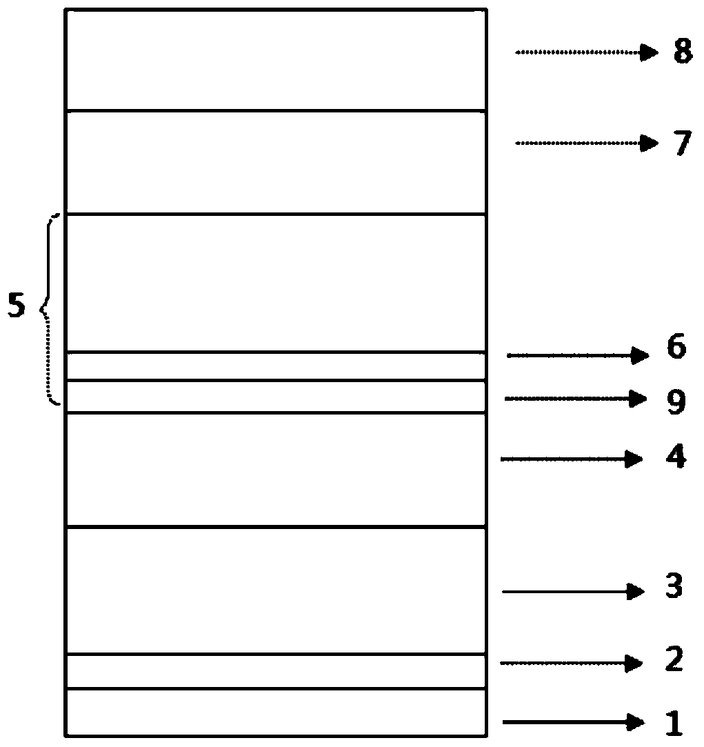
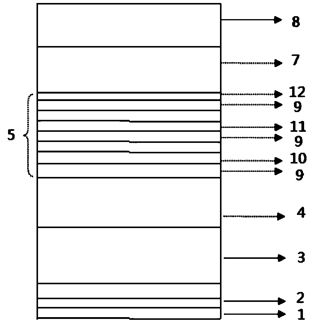
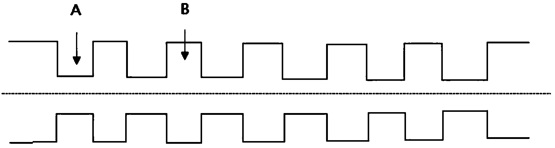
[0042] The invention uses Aixtron MOCVD to grow high-brightness GaN-based LED epitaxial wafers. Using high-purity H 2 or high purity N 2 or high purity H 2 and high purity N 2 The mixed gas as the carrier gas, high-purity NH 3 As the N source, the metal-organic sources trimethylgallium (TMGa) and triethylgallium (TEGa) are used as the gallium source, trimethylindium (TMIn) is used as the indium source, and the N-type dopant is silane (SiH 4 ), trimethylaluminum (TMAl) as the source of aluminum, and the P-type dopant as magnesocene (CP 2 Mg), the substrate is (0001) sapphire, and the reaction pressure is between 100mbar and 800mbar. The specific growth method is as follows (for the epitaxial structure, please refer to figure 2 , please refer to the energy band in step 5 Figure 4 ):

[0043] 1. Treat the sapphire substrate at a high temperature for 8-10 minutes in a hydrogen atmosphere at 1000-1100°C;

[0044] 2. Lower the temperature to 540-590°C, and grow a low-temp...


PUM


Abstract

The invention provides an epitaxial growth method of a light-emitting diode (LED) structure including a potential barrier with gradually-varied thickness. The light-emitting layer multiple quantum well (MQW) growing step is that H2 and / or N2 serve / serves as carrier gas, an In-doped InxGa(1-x)N layer with the 2.5-3nm thickness grows in a reaction chamber with the 730-750 DEG C temperature and the 100-800mbar pressure, wherein x=0.20-0.21; the temperature of the reaction chamber is adjusted to be 800-840 DEG C, trimethyl gallium is led into the reaction chamber for a time period R, and a first GaN layer with the thickness D grows; an InGaN layer grows repeatedly, trimethyl gallium is led into the reaction chamber for 0.75-0.95 time of a time period R, and a second GaN layer with the 0.75-0.95 times of thickness D grows; by the analogy, the thickness of the GaN layers is gradually decreased layer by layer. The GaN thickness of a light-emitting layer is changed and gradually decreased, accordingly distribution of electrons and electron holes is improved, and the LED lighting effect is improved.

Description

technical field [0001] The invention relates to the field of LED epitaxial design, in particular to an LED structure epitaxial growth method and its structure including gradient thickness epitaxy. Background technique [0002] At present, the domestic MOCVD growth of LED epitaxial layer involves the growth of the light-emitting layer. Most of them are potential well InGaN and potential epitaxial GaN. [0003] The thickness of the light-emitting layer is generally controlled at 150nm-250nm. Compared with N and P-type GaN, the resistance of the light-emitting layer is relatively high; the resistance of the light-emitting layer. [0004] The advantage of higher resistance value: the light-emitting layer is close to the structure of the N layer, and the GaN resistance value is high and can block most electrons, and the electron concentration value is 1E+20-2E+20 / cm 3 (The mobility of electrons in N-type GaN is as high as 200-250v / cm 2 , the Si dopant ionizes more than 90%, th...

Claims


Application Information

Patent Timeline
Patent Type & Authority Applications(China)
IPC IPC(8): H01L33/06H01L33/00
Inventor 赵云林传强
Owner XIANGNENG HUALEI OPTOELECTRONICS
Why Eureka
Try Eureka